Key Overview
Who this is for: System integrators and OEM buyers who need a fully customizable wireless bridge PCBA solution with detailed technical specifications, production-ready documentation, and validated reference designs.
Core Issue: Off-the-shelf wireless bridge PCBAs built on one-size-fits-all designs cannot match specialized industry demands — either performance overhead drives up costs unnecessarily, critical specs fall short, or hardware fails in real-world conditions. Buyers need a standardized yet flexible approach from requirements through production delivery.
Key Conclusions: This end-to-end PCBA customization solution covers the complete lifecycle: (1) hardware architecture design (chipset selection, RF front-end tuning, interface configuration), (2) firmware and software customization (driver tuning, protocol stack optimization, management UI), (3) environmental validation (temperature chamber testing, vibration/shock, IP rating certification), (4) production integration (SMT assembly, QA, logistics). Based on validated reference designs covering WiFi 5/6/7, dual-band, and high-power FEM configurations for security surveillance, smart campuses, outdoor private networks, and industrial IoT.
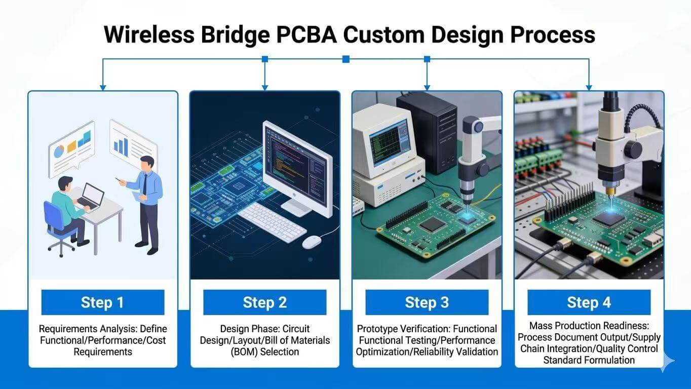
As IoT, security surveillance, smart campuses, and outdoor private networks continue to expand, the wireless bridge has become the backbone of wireless data transmission. Its performance, stability, and environmental adaptability directly determine whether a transmission system delivers on its promises. Off-the-shelf wireless bridge PCBAs, built around a one-size-fits-all design philosophy, simply can’t keep up with the specialized demands of different industries and use cases. The result: either performance overhead drives up costs unnecessarily, critical specs fall short and block deployment, or the hardware can’t handle real-world conditions and fails repeatedly. That’s exactly why we built this practical, highly adaptable, cost-effective Wireless Bridge PCBA Customization Solution. From requirements scoping through production delivery, every step follows a standardized, detailed process that balances technical feasibility with real-world execution.
1. Industry Pain Points (Where Off-the-Shelf Solutions Fall Short)
The limitations of generic wireless bridge PCBAs go far deeper than most buyers realize. These aren’t minor inconveniences — they’re the reason so many projects stall, overrun budgets, or fail outright. Here’s what we hear from customers who come to us for a better approach:
Poor Scenario Fit Means the Hardware Simply Won’t Work
Different deployment environments impose wildly different requirements on a wireless bridge PCBA — and generic boards can’t stretch far enough to cover them all:
- Outdoor Long-Haul (Forest Fire Prevention, Mountain Surveillance): Standard PCBA RF power tops out at ≤20dBm, capping transmission distance at about 10km — nowhere near enough for wide-area monitoring. No low-temperature preheat circuit means the board won’t even start below -20°C, leading to frequent outages in winter.
- High-Interference Environments (Ports, Factories, Substations): Generic boards use basic filtering, with an Adjacent Channel Rejection Ratio (ACRR) of ≤45dB. In practice, that means packet loss hits 15% or higher — unacceptable for real-time HD video (1080p and above) backhaul.
- High Salt Spray / High Humidity (Coastal Ports, Islands): Off-the-shelf PCBs skip conformal coating and keep gold plating under ≤1µm. After six months in a marine environment, you’re looking at corrosion and shorts — and failure rates climb past 30%.
- Low-Power / Solar-Powered (Remote, Unattended Sites): Standard PCBAs have no intelligent power management. Idle power consumption sits at ≥5W, which means a solar + battery setup can’t sustain 24/7 operation — defeating the purpose of a self-powered deployment.
Performance and Cost Are Out of Balance — Poor Value All Around
To cast a wide net, general-purpose PCBAs pack in a ton of features most projects don’t need — multi-band support, extra interfaces, the works. That creates two problems. First, you end up paying 25–35% more for capabilities you’ll never use, stretching an already tight project budget. Second, the extra circuitry pushes total power draw to ≥8W, which drives up long-term operating costs (power supply, heat dissipation) and eats up valuable board real estate — making it impossible to fit the PCBA into compact enclosures like mini surveillance bridge housings.
Minimal Technical Support Means Timelines Slip Out of Control
Most PCBA vendors sell standard products and nothing else. No customization, no integration support. Once you receive the boards, you’re on your own to figure out antenna matching, enclosure fit, and power system compatibility. That adds weeks or months of engineering work, drives up internal R&D costs, and introduces compatibility failures that can derail the entire project. We’ve seen deployment timelines stretch by 1–2 months — and sometimes the solution never recovers.
Non-Compliant Designs Fail Certification — and Kill Project Acceptance
Regulated industries — security, energy, government — demand strict compliance certifications (CE, FCC, RoHS) for wireless bridge PCBAs. Generic boards frequently fail these tests because their circuit designs cut corners on emissions, safety margins, or materials. When certification fails, project acceptance stalls and the financial hit can be significant.
2. Our Customization Philosophy (No Bloat, Just Precision)
Here’s how we think about customization: start with what the customer actually needs to make the project work, design within the bounds of what’s technically feasible, and keep cost firmly in view. We don’t do “customization for customization’s sake.” Every design decision maps directly to a real-world requirement and a practical execution path. And yes — we also make sure the content maps to high-intent search terms like “Wireless Bridge PCBA Customization Parameters,” “Implementation Cycle,” and “Cost Control,” so customers can find this solution fast and use it as a working reference.
The principles are straightforward: match parameters precisely to the deployment scenario, follow a standardized process from end to end, keep costs transparent and predictable, and provide full post-sales support. Every step — from design through production — is traceable and auditable. Our customers don’t need to invest extra engineering resources to make the solution work.
3. The Full Customization Process: From Requirements to Production
We’ve broken the process into six stages — from initial requirements gathering all the way through volume production. Each stage comes with clear execution criteria, defined responsibilities, milestones, and acceptance checkpoints. The goal: make the entire workflow repeatable and transparent, so every customer knows exactly what to expect.
Stage 1: Deep-Dive Requirements Assessment (1–3 Business Days — Get It Right Upfront)
Core Objective: Fully unpack the customer’s requirements — identifying the “must-hit” parameters, the “nice-to-haves,” and the “must-avoid” failure modes — and produce an actionable Requirements Assessment Report. This report becomes the single source of truth for design, testing, and delivery, eliminating the misalignment that plagues projects with vague or incomplete specs.
Requirements Gathering (1–3 Business Days)
Using a combination of site surveys, remote meetings, and document reviews, we collect requirements across seven critical categories:
| Category | What We Collect (Actionable, Quantified) | Example (Varies by Scenario) |
|---|---|---|
| Deployment Environment | Transmission distance, obstructions (none / light / heavy), RF interference levels, temperature range, humidity, salt spray exposure, available enclosure space | Forest Fire Prevention: 35km clear LoS, 25km with light tree occlusion, -40°C to +75°C, salt spray ≥1000h, board space ≤80×60mm |
| Performance Specs | RF output power, throughput, packet loss, latency, frequency band (2.4 / 5.8 / dual), ACRR, Rx sensitivity | Port Surveillance: 27dBm RF power, ≥1.2Gbps throughput, ≤0.1% packet loss, ≤20ms latency, 5.8GHz, ACRR ≥60dB |
| Power | Power source (mains / solar / DC), input voltage range, power consumption (active / idle / standby), protection requirements | Remote Solar: 9–36V DC input, active ≤5W, idle ≤2W, overvoltage / overcurrent / short-circuit protection required |
| Mechanical | PCB dimensions, thickness, mounting type (SMD / DIP), connectors (RJ45 / serial / USB), component layout constraints | Compact Surveillance Bridge: 50×40mm PCB, 1.6mm thickness, SMD, single Gigabit port, layout must avoid enclosure vent openings |
| Compliance | Required certifications (CE / FCC / RoHS, etc.), environmental standards, safety codes | EU / US Export: CE + FCC certified, RoHS 2.0, circuit meets IEC 60950-1 |
| Budget | Target unit cost, expected order volume (≥1K / ≥5K), cost-reduction goals | 5K units, target ≤$12/unit, goal: 25% below equivalent off-the-shelf solution |
| Timeline | Prototype lead time, test window, production delivery schedule, expedite capability | Prototype in 1–5 days, testing 2–5 days, production 7–15 days; expedite to 3-day prototype available |
Requirements Analysis & Prioritization (2 Business Days)
Our engineering team breaks down, validates, and refines every requirement, tagging each one as Core (must-have), Secondary (optimization opportunity), or Infeasible (alternative proposed). Example: if a customer asks for “50km range at ≤3W,” that’s physically unrealistic with today’s RF tech. We’d come back with “≤6W at 50km” or “≤3W at 40km” as viable alternatives — keeping the solution grounded in reality and preventing disputes later.
Requirements Assessment Report (2 Business Days)
The final report covers five sections and is jointly signed as the baseline for all downstream work: ① Deployment environment analysis; ② Agreed parameter table; ③ Preliminary cost estimate; ④ Proposed delivery timeline; ⑤ Risk register with mitigation plans (e.g., supply chain constraints, test failures).
Stage 2: Solution Design (1–5 Business Days — Where Performance Meets Compliance)
With the Requirements Assessment Report as our blueprint, our hardware, RF, and software engineering teams work in parallel. We use simulation tools and multi-option comparison to validate every design choice before committing to silicon — eliminating rework and managing cost from the start. The output is a complete design package covering schematics, layout, BOM, and compliance analysis.
Hardware Circuit Design (2 Business Days)
We focus on three core circuit blocks — prioritizing compliance, cost efficiency, and scenario fit. Every component is specified with model number, key parameters, and placement guidance to avoid unnecessary redundancy:
RF Front-End (The Backbone of Transmission Performance)
The RF chain is designed from the ground up based on range and frequency band requirements. Every parameter is quantified and verifiable:
- Chipset Selection: We pair high-linearity, power-efficient SoCs (e.g., Qualcomm QCA9558, MediaTek MT7621) with the right external PA (e.g., SKY85713 for 27dBm output). The goal: stable RF performance without overspending on silicon we don’t need.
- Antenna Matching Network: Custom LC matching tunes the impedance to a precise 50Ω, maximizing antenna gain and minimizing return loss. For long-haul links (≥30km), we use high-gain antenna matching to keep signal loss under 10%.
- Filtering & Interference Rejection: For electrically noisy environments (ports, factories), we integrate high-order bandpass filters and optimize the layout to push ACRR past 60dB — cutting packet loss to under 0.1% and keeping HD video feeds stable.
- Compliance by Design: The RF path is designed from the start with CE and FCC emission limits in mind — harmonic filtering, spurious suppression, and conducted emission control are built into the layout, not bolted on after the fact. This cuts certification risk and avoids expensive late-stage redesigns.
Power Management Circuitry (Active Power Optimization)
Power design is adapted to the deployment scenario, not capped by a generic spec:
- Solar / Battery Scenarios: We use high-efficiency DCDC converters (≥92% efficiency) and implement intelligent sleep/wake scheduling. Active power can be brought down to ≤5W, idle to ≤2W — making 24/7 solar operation realistic.
- Grid-Powered Scenarios: Cost takes priority. We use mainstream converter ICs, drop the sleep-mode complexity, and target 6–8W active power with basic protection (overvoltage, reverse polarity).
- Wide Input Range (9–48V DC): Many industrial sites (substations, factories) have unstable supply voltage. We support extended input range with transient protection to prevent field failures.
Protection & Environmental Hardening
Environmental threats are handled at the board level, not left to the enclosure:
- Conformal Coating: Coastal and industrial deployments get full acrylic or silicone conformal coating as standard, protecting against salt spray, humidity, and conductive dust.
- Gold Plating (≥3µm): Critical connectors and contact pads get thicker gold plating — especially important for marine environments where corrosion resistance is make-or-break.
- Thermal Management: For high-power RF designs (27dBm+), we route dedicated thermal vias, add copper pours, and specify thermal pads in the layout — keeping junction temperatures within safe limits at +75°C ambient.
PCB Layout Design (2 Business Days)
Layout is purpose-built for the target enclosure and scenario, not a generic reference design:
- Compact Form Factors: For space-constrained designs (e.g., mini surveillance bridges, drones), we optimize component density and use multi-layer boards (4–6 layers) to shrink the footprint to 50×40mm or smaller.
- RF-Aware Layout: Critical RF traces are impedance-controlled (50Ω), isolated from noisy digital lines, and kept as short as practical. PA stages are spaced from sensitive receiver chains to prevent desense.
- Thermal & Mechanical Fit: We model the board in 3D against the customer’s enclosure drawings, verifying mounting hole locations, connector positions, and keep-out zones before tape-out.
BOM & Cost Optimization (1 Business Day)
With the design frozen, we optimize the Bill of Materials for cost without cutting corners on reliability:
- Multi-Source Verification: Every component on the BOM is verified against 2–3 qualified alternate suppliers, reducing supply chain risk and creating price leverage.
- Cost vs. Reliability Trade-offs: We document every cost-reduction decision — e.g., switching from a premium brand inductor to a reputable mid-tier equivalent — along with the impact assessment, so the customer can make an informed call.
- Volume Pricing Tiers: The BOM includes pricing at three order volumes (1K, 5K, 10K), so customers can plan for scale.
Stage 3: Rapid Prototyping (1–5 Business Days — Hardware in Your Hands, Fast)
Once the design package is signed off, we move immediately to prototyping:
- Standard Prototype: 5–10 fully assembled boards delivered in 5 business days. Includes solder paste inspection (SPI), AOI, and first-article functional test.
- Expedited Prototype: Need boards in 3 days? We can compress the SMT and assembly queue with priority scheduling.
- Deliverables: Assembled boards + manufacturing files (Gerber, pick-and-place, BOM) + preliminary test report.
Stage 4: Full Functional & Environmental Testing (2–5 Business Days — No Surprises at Deployment)
Every prototype goes through a structured test plan aligned to the Requirements Assessment Report. Tests are grouped into three categories:
- RF Performance: Output power, Rx sensitivity, ACRR, EVM, spectral mask — verified across the full operating temperature range using calibrated chamber equipment.
- Environmental Stress: Temperature cycling (-40°C to +85°C), humidity soak (85% RH, 85°C, 1000h), salt spray (ASTM B117, 48–1000h depending on rating), and mechanical shock/vibration per IEC 60068-2.
- System Integration: Actual throughput benchmark (iPerf), latency under load, packet loss at maximum range, and compatibility test with the customer’s antenna and enclosure.
Test results are documented in a formal report with pass/fail status for every requirement. Any failure triggers a root-cause analysis and a documented rework cycle before the next prototype spin.
Stage 5: Small-Batch Trial Run & Process Validation (5–7 Business Days)
Before committing to full production, we run a pilot batch of 50–200 units through the actual SMT line:
- Process Verification: Solder paste deposition, reflow profile, AOI coverage, and first-pass yield are measured and compared against targets.
- Statistical Sampling: A random sample from the pilot batch (per ANSI/ASQ Z1.4) undergoes full functional and environmental retest to confirm the design is production-ready.
- Process Adjustments: Any yield issues trigger corrective action — stencil redesign, reflow profile tuning, or placement optimization — before production ramp.
Stage 6: Volume Production & Logistics (7–15 Business Days — On-Time Delivery, Every Time)
Once the pilot batch is qualified, full production kicks off:
- Production Capacity: Standard lead time is 7–15 business days for quantities up to 10K units. Higher volumes can be staged across multiple production windows.
- Quality Gates: Every board gets SPI + AOI. A statistically sampled subset (per agreed AQL) gets full functional test. Any lot that doesn’t meet the agreed yield threshold is held for review.
- Packaging & Logistics: Boards are shipped in anti-static packaging with moisture barrier bags. We support air freight (DDP, DAP) and sea freight, with full tracking and documentation (packing list, invoice, COO).
5. Ready to Talk?
This isn’t theoretical. Here’s what sets this solution apart from working with a standard PCBA vendor:
- Single-Point Accountability: One engineering team handles everything — requirements, design, prototyping, testing, and production. No finger-pointing between a design house and a fab.
- Documented Traceability: Every requirement is linked to a test case. Every design decision is documented. Every test result is recorded. No black boxes.
- Cost Transparency: You see the BOM with real component pricing. You see where costs are concentrated and where trade-offs can be made — you’re in control, not guessing.
- Built for Scale: The design isn’t just a prototype. It’s optimized from day one for volume manufacturing — standard components, mature processes, and testable at scale.
5. Ready to Talk?
If you’re evaluating a wireless bridge PCBA for your next project — or you’ve hit a wall with off-the-shelf boards — we’d like to hear about it. Send us your requirements and we’ll come back with a feasibility assessment and a preliminary budget within 3 business days.
No pressure. No upsells. Just a straight answer about whether we can help — and if we can, what it’ll take.