Industrial Wireless PCBA Customization: Design & Manufacturing Guide
Blog 2026-06-14
Industrial Wireless PCBA Customization: Services, Quality Control & Cost Optimization
Key Overview
Target Audience: Industrial wireless device manufacturers, OEM/ODM procurement decision-makers, electronics engineers, product development managers
Core Question: What PCBA customization services do industrial wireless devices need? How to ensure PCBA quality meets industrial standards? How to optimize customization costs?
Key Conclusion: Industrial wireless PCBA customization requires full-process services from design, component selection, firmware development to testing and certification, following IPC-A-610 Class 3 standards, with cost control achieved through DFM optimization and volume procurement.
PCBA Customization Services for Industrial Wireless Devices
Industrial wireless devices demand fundamentally different PCBA design approaches compared to consumer electronics. A consumer WiFi router PCB might operate reliably for 2-3 years in a climate-controlled home, while an industrial wireless bridge PCBA must function for 5-10 years in environments ranging from -40°C arctic cold to +85°C desert heat, with continuous exposure to vibration, moisture, and electromagnetic interference. This difference in operating conditions drives every aspect of the PCBA customization process — from layer stackup design to component selection to assembly quality standards.
The following sections detail the four pillars of industrial wireless PCBA customization. Each pillar represents a critical decision point where the choices made by the design team directly determine the final product’s performance envelope, manufacturing cost, and long-term reliability.
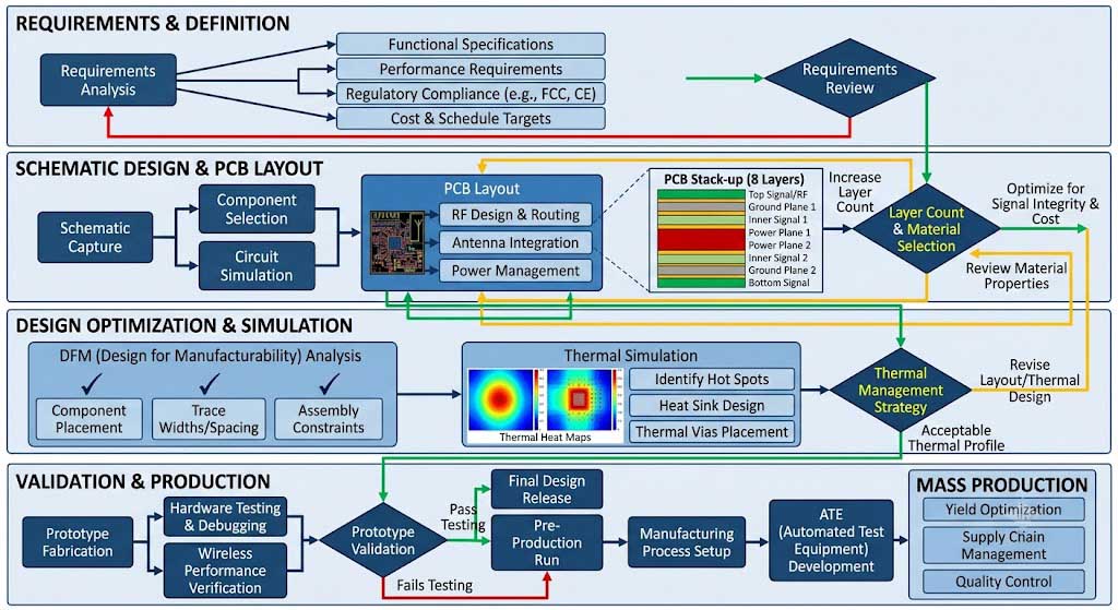
Design Customization
PCBA design for industrial wireless devices must balance RF performance, thermal management, and mechanical robustness within the constraints of the target form factor. The layer count decision is the starting point: 2-layer boards are sufficient for simple wireless bridges with basic power and signal routing, while 8-12 layer boards are required for devices integrating WiFi 6/6G chipsets, multiple Ethernet ports, PoE power management, and peripheral interfaces. Each additional layer pair adds approximately 15-20% to the PCBA fabrication cost but provides dedicated ground planes that improve RF performance and signal integrity.
Material selection is equally critical. Standard FR-4 is adequate for basic designs operating below 2.4 GHz, but high-frequency laminates such as Rogers 4003C or Isola FR408 are required for 5 GHz and 6 GHz wireless bridges. These materials have controlled dielectric constants (Dk) and low dissipation factors (Df), ensuring consistent RF impedance across the board and minimizing signal loss in the RF trace routing. The cost difference is significant — high-frequency laminates cost 2-4 times more than FR-4 — but for a wireless bridge that must maintain 500 Mbps throughput at 10 km range, the RF performance loss from using FR-4 would be unacceptable.
Thermal management is the third critical design consideration. The main chipset on a wireless bridge PCBA — typically consuming 8-15W depending on the standard — generates heat that must be conducted away from sensitive components. Without proper thermal design, a 10°C increase in junction temperature can reduce chipset lifespan by 50% and cause frequency drift in the RF oscillators that degrades link performance. Common thermal solutions include copper pour planes for heat spreading, thermal vias under high-power ICs, and provision for heatsink attachment via the enclosure design. For outdoor bridges deployed in direct sunlight, the thermal design must account for both self-heating and solar radiation, which can add 15-25°C to the ambient temperature.
Component Selection and Sourcing
Component selection is where the difference between a commercial-grade and industrial-grade PCBA is determined — often by specific component variants that look identical but have dramatically different temperature ratings and reliability specifications. An MLCC capacitor rated for 85°C maximum operating temperature costs $0.02, while the same capacitance value with X7R dielectric rated for 125°C costs $0.08. For a PCBA with 200 capacitors, the 4x cost difference adds up, but using the lower-rated parts in an outdoor wireless bridge would lead to premature failure as the capacitors’ capacitance drifts outside specification at high temperatures, causing power supply ripple and eventual system instability.
Supply chain security has become a critical concern for industrial PCBA production. The semiconductor shortages of 2021-2023 demonstrated that reliance on a single source for key components — such as the main wireless chipset, PoE controller, or Ethernet PHY — can halt production for 6-12 months. Industrial PCBA customization should include a formal component engineering process that identifies at least two approved alternate components for each critical part. These alternates must be pre-qualified in the design, with their electrical and thermal characteristics verified so that they can be substituted without re-design. This approach adds upfront engineering cost but provides production resilience that prevents costly manufacturing delays.
RoHS and REACH compliance are mandatory for products sold in the EU and increasingly required globally. However, industrial applications sometimes require exemptions for specific lead-containing solders or components that have no RoHS-compliant equivalent with the required reliability. For example, high-temperature solders used in power stages may require lead content to prevent thermal fatigue cracking. A qualified PCBA customization partner should understand these exemptions and advise on when they apply, rather than taking a rigid “RoHS always” approach that could compromise product reliability.
Firmware and Software Customization
The firmware layer is what transforms a generic wireless chipset reference design into a purpose-built industrial wireless bridge with specific performance characteristics and management capabilities. Off-the-shelf reference firmware from the chipset vendor typically provides basic WiFi functionality with generic configuration options. Custom firmware development is required to implement features that differentiate the product for industrial use: proprietary TDMA protocols for deterministic latency, custom QoS algorithms for video prioritization, SNMP MIB extensions for integration with network management systems, and secure boot mechanisms that prevent unauthorized firmware modifications.
Linux and OpenWrt are the dominant operating system platforms for industrial wireless bridge development. OpenWrt provides a mature networking stack with support for advanced features like mesh networking, VLAN segmentation, and dynamic routing protocols (OSPF, BGP). The customization effort typically involves: porting the chipset driver to the target kernel version; developing a hardware abstraction layer for the specific PCBA peripherals (GPIOs, LEDs, watchdogs); implementing the web-based management interface; and integrating with cloud management platforms if remote device management is required. A typical firmware customization project for a new wireless bridge PCBA requires 4-8 weeks of engineering effort, depending on the complexity of the feature set.
Protocol support extends beyond standard WiFi to include industrial IoT protocols. A wireless bridge may need to simultaneously handle WiFi client connections, Bluetooth Low Energy (BLE) for proximity sensors, Zigbee for mesh sensor networks, and LoRa for long-range low-power sensor backhaul. Integrating multiple wireless protocols on a single PCBA requires careful RF coexistence planning — simultaneous 2.4 GHz WiFi and BLE operation, for example, can cause desensitization of the BLE receiver by the much higher WiFi transmit power. The firmware must implement time-division multiplexing (TDM) or adaptive frequency hopping to prevent collisions between protocols operating in the same frequency band.
Testing and Certification Support
Testing for industrial wireless PCBA is not a single step but a continuous process spanning design validation, regulatory certification, and production quality assurance. Each testing phase addresses specific risks and requires different equipment, methodologies, and pass/fail criteria. Skipping or shortening any testing phase increases the risk of field failures that are 10-100 times more costly to fix than catching the issue during development.
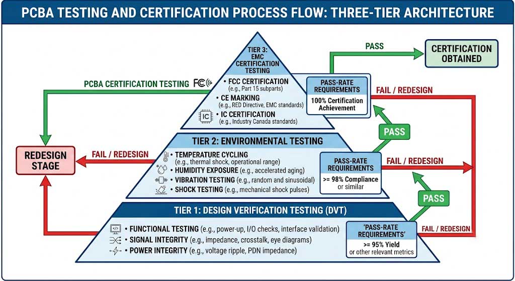
| Service | Description |
|---|---|
| Design verification testing | Functional testing, signal integrity, power integrity |
| Environmental testing | Temperature cycling, humidity, vibration, shock |
| EMC testing | EMI/EMC compliance, FCC, CE, IC certifications |
| Production testing | ICT, FCT, burn-in testing |
Design verification testing (DVT) is the first and most critical testing phase. Before any regulatory testing or production commitment, the PCBA design must be validated for basic functionality: power supply voltages at all test points within specification; RF output power, frequency accuracy, and EVM (Error Vector Magnitude) meeting the chipset datasheet specifications; Ethernet PHY link quality and signal integrity on all ports; and all GPIOs, LEDs, and interfaces functioning correctly. DVT typically takes 1-2 weeks and is performed on 5-10 prototype boards. Any design issues found at this stage are corrected with a board spin before proceeding to formal testing.
Environmental testing validates the PCBA’s ability to survive and operate in the target deployment environment. Temperature cycling from -40°C to +85°C for 100+ cycles tests solder joint reliability and component thermal stress tolerance. Humidity testing at 95% relative humidity and 50°C for 48 hours checks for moisture ingress and corrosion susceptibility. Vibration testing at 5-500 Hz with 2G acceleration simulates the mechanical stress from nearby industrial machinery. Each environmental test has specific pass criteria: no functional failures during the test, no physical damage after the test, and parametric measurements (RF power, frequency, sensitivity) remaining within specification after the test.
EMC testing is required for regulatory certification (FCC Part 15 in the US, CE RED in the EU, IC RSS-210 in Canada). This testing measures both conducted and radiated emissions from the PCBA to ensure they stay within legal limits, as well as immunity to external electromagnetic fields. A typical EMC test campaign for a wireless bridge PCBA costs $15,000-30,000 depending on the number of test configurations and the laboratories’ hourly rates. Designing for EMC compliance from the start — with proper shielding, filtering, and layout practices — is significantly more cost-effective than trying to fix EMC issues after the design is complete, which often requires costly board respins and additional testing rounds.
Quality Control Standards for Wireless PCBA
Quality control for industrial wireless PCBA is fundamentally different from consumer electronics quality assurance. In consumer products, a 1% field failure rate might be acceptable — the cost of replacing a few units under warranty is less than the cost of additional testing. In industrial wireless bridge deployments, a single field failure can require a technician to drive 200 km to a remote pipeline inspection point, costing $500-2,000 in travel and labor alone. For a deployment of 100 bridges supporting mission-critical monitoring, even a 1% failure rate creates unacceptable operational risk. This economic reality drives industrial PCBA quality standards to target defect rates measured in parts per million (PPM) rather than percentages.
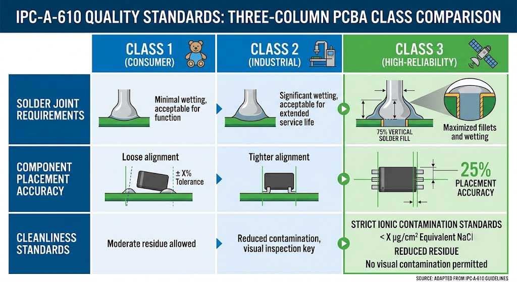
IPC-A-610 Class 3 Standards
IPC-A-610 Class 3 is the highest reliability classification for electronic assembly, designed for applications where equipment failure would cause significant operational disruption or safety hazards. The standard defines specific acceptance criteria for every aspect of PCBA assembly, from solder joint fillet geometry to component placement accuracy to board cleanliness. Class 3 acceptance is not a single test — it is a comprehensive inspection framework that covers hundreds of specific criteria, each with defined pass/fail limits and measurement methods.
Solder joint quality under Class 3 requires 75% minimum vertical fill for through-hole components (compared to 50% for Class 2) and 100% side wetting for surface-mount components. The solder fillet must show a smooth, concave profile indicating proper wetting of both the component termination and the PCB pad. Any evidence of cold solder joints, insufficient wetting, or excessive solder that could create bridging between adjacent pins is a rejection condition. These criteria are verified through automated optical inspection (AOI) on every board produced, with AOI machines checking each solder joint against the Class 3 reference images at rates of 50-100 joints per second.
Component placement accuracy for Class 3 requires significantly tighter tolerances than lower classes. A surface-mount resistor must be centered on its pads within 25% of the pad width in both X and Y axes, with no tombstoning (one end lifted off the pad) or skew beyond specification. For fine-pitch ICs with 0.5 mm or smaller pin pitch, the placement accuracy requirement is particularly stringent — even a 0.1 mm misalignment can create solder bridges between adjacent pins that cause short circuits. These tight tolerances require high-precision pick-and-place machines with vision alignment systems and regular calibration verification.
Cleanliness standards under Class 3 require that the fully assembled PCBA be free of flux residue, solder balls, dust particles, and any other contaminants. This is achieved through a multi-stage cleaning process using deionized water, saponifiers, and ultrasonic agitation, followed by ionic contamination testing that measures the conductivity of a rinse solution against a maximum allowable threshold. For industrial wireless bridges deployed in high-humidity environments, cleanliness is particularly critical — residual flux can absorb moisture and create conductive paths that cause leakage currents and electrochemical migration, eventually leading to short circuits and board failure.
ISO 9001 Quality Management
ISO 9001 certification provides the process framework that ensures quality consistency across production runs, not just for individual boards. While IPC-A-610 defines what a quality board looks like, ISO 9001 defines the management system that ensures every board in every production run meets those standards consistently. The certification requires documented procedures for every quality-critical process, from incoming material inspection through assembly, testing, and shipping.
Process control under ISO 9001 requires that all production equipment — solder paste printers, pick-and-place machines, reflow ovens, wave solder machines, and inspection systems — have documented calibration schedules, preventive maintenance procedures, and process qualification records. For example, the reflow oven temperature profile must be verified at the start of each production shift using a thermocouple-equipped test board that travels through the oven with the production boards. If the measured profile deviates from the qualified specification by more than 3°C at any zone, production must be stopped until the oven is recalibrated. These controls prevent the gradual process drift that can cause quality issues even when individual board inspections appear acceptable.
Continuous improvement is enforced through the ISO 9001 requirement for corrective action reporting. Any quality issue — whether identified through incoming inspection, in-process testing, final inspection, or customer feedback — must be documented with root cause analysis, corrective action, and verification of effectiveness. Over time, this creates a quality knowledge base that drives continuous improvement in both the product design and the manufacturing process. For a PCBA manufacturer producing wireless bridge boards, common corrective actions might include: adding additional test coverage for a specific failure mode, updating the solder paste stencil design to prevent a recurring solder defect, or requalifying a component supplier whose parts showed higher than acceptable defect rates.
In-Circuit Testing (ICT) and Functional Testing
ICT and FCT serve complementary roles in the production testing strategy: ICT verifies that the board was assembled correctly, while FCT verifies that the board functions correctly in its intended application. Together, they provide comprehensive defect coverage that catches approximately 95-98% of all potential manufacturing defects before the board ships to the customer.
| Test Type | Purpose | Coverage |
|---|---|---|
| In-Circuit Testing (ICT) | Verify component placement and solder connections | 99% of solder joints and components |
| Functional Testing (FCT) | Verify overall board functionality | Full functional verification |
| Boundary Scan | Test complex IC connections | High-density interconnects |
| Burn-In Testing | Identify early failures under stress | High-reliability applications |
In-Circuit Testing uses a bed-of-nails fixture that makes contact with every net on the PCBA through dedicated test points. The ICT system measures resistance, capacitance, and diode characteristics at each test point, comparing measured values against the design specification. A missing component, wrong value component, or poorly soldered connection is detected immediately. ICT can test a typical wireless bridge PCBA in 30-60 seconds, providing 99% coverage of all components and solder joints. The limitation of ICT is that it tests individual components in isolation but cannot verify that the board performs its intended function under real operating conditions.
Functional Testing fills this gap by powering up the PCBA and running a comprehensive test sequence that simulates actual operation. For a wireless bridge PCBA, FCT typically includes: verifying that the board boots and loads firmware correctly; testing all Ethernet ports for link establishment and packet transmission at gigabit speeds; measuring RF output power, frequency accuracy, and modulation quality on all supported bands; verifying WiFi client association and data throughput; and checking all user interface elements (LEDs, buttons, serial console). FCT takes 2-5 minutes per board depending on the test coverage depth, providing confidence that the board is fully functional before shipping. The combination of ICT (component-level verification) and FCT (system-level verification) provides the comprehensive quality assurance required for industrial wireless bridge PCBA.
Environmental Stress Screening
Environmental stress screening (ESS) identifies latent defects that would not be caught by ICT or FCT but would cause premature failure in the field. These defects include: cracked component packages from thermal stress during soldering; weak wire bonds in IC packages that fail under vibration; and contaminant particles that cause intermittent shorts under temperature cycling. ESS applies accelerated stress conditions that trigger these latent defects to fail during the screening process rather than in the field.
Temperature cycling from -40°C to +85°C for 20-100 cycles is the most common ESS for industrial wireless PCBA. Each cycle exposes the board to the extreme temperature gradient of 15-20°C per minute, causing differential thermal expansion between components, solder joints, and the PCB substrate. Components with cracked packages or weak solder joints will typically fail within the first 20 temperature cycles. For the highest reliability applications, 100+ cycles may be specified, with functional testing performed at both temperature extremes to verify operation across the full temperature range.
Vibration testing per MIL-STD-810 applies random vibration in the 5-500 Hz range with 2-5G acceleration, simulating the mechanical stress of transportation and operation near industrial machinery. The board is mounted on a vibration shaker and subjected to 15-30 minutes of random vibration in each of three axes (X, Y, Z). After vibration, a full functional test is performed to verify that no connections have loosened and no components have cracked. For wireless bridges deployed near pipelines with pump stations or compressor stations, vibration screening is particularly important, as these environments have continuous low-frequency vibration that can gradually fatigue solder joints over months of operation.
Cost Optimization Strategies for Industrial Wireless PCBA
Cost optimization for industrial PCBA is fundamentally different from cost reduction in consumer electronics. In consumer products, cost reduction often means switching to lower-grade components, reducing test coverage, or using cheaper PCB materials — all of which would be unacceptable for industrial wireless bridges where reliability directly impacts operational costs. Effective cost optimization for industrial PCBA focuses on reducing manufacturing waste, improving yield, and negotiating better prices through volume commitments, rather than compromising on materials or workmanship.
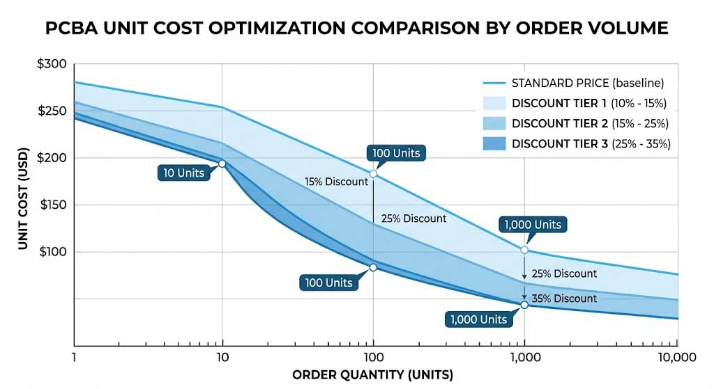
Volume-Based Pricing Models
PCBA pricing follows a power-law relationship with volume: doubling the order quantity typically reduces the per-unit price by 10-15%. This price reduction comes from three sources: component procurement discounts (the largest factor at 50-60% of total savings), manufacturing setup amortization (20-30%), and learning-curve efficiency improvements (10-20%). Understanding this breakdown helps in structuring procurement agreements that maximize savings without over-committing to inventory.
| Order Volume | Typical Price Reduction | Lead Time |
|---|---|---|
| 1-100 units | Standard price | 2-4 weeks |
| 100-1,000 units | 10-15% | 3-5 weeks |
| 1,000-10,000 units | 15-25% | 4-6 weeks |
| 10,000+ units | 25-35% | 6-8 weeks |
The most effective cost optimization strategy for volume-based pricing is a phased volume commitment. Rather than ordering 10,000 units at once (which requires significant upfront capital and inventory carrying costs), a phased agreement commits to 10,000 units over 12-18 months with scheduled releases of 500-1,000 units per month. The PCBA manufacturer can use the total committed volume to negotiate component pricing with suppliers, while the buyer avoids the cash flow and inventory risk of a single large order. This approach typically achieves 80-90% of the volume discount available from a single order, with significantly less financial risk.
Component Cost Reduction Techniques
Component cost is the largest single element of PCBA pricing, typically accounting for 50-70% of the total board cost. Strategic component selection and sourcing can reduce this cost by 15-25% without changing the board design or compromising performance. The key is understanding which components contribute most to the BOM cost and having a systematic approach to optimizing those line items.
Alternate component sourcing is the most direct cost reduction technique. For many component categories — resistors, capacitors, inductors, and basic semiconductors — there are multiple qualified suppliers offering functionally equivalent parts at different price points. A formal alternate component qualification process identifies 2-3 approved sources for each critical component, with documented testing confirming that the alternate parts meet all electrical, thermal, and reliability requirements. The purchasing team can then bid the annual volume across qualified suppliers and select the most cost-effective option. This approach typically reduces passive component costs by 15-25% and semiconductor costs by 5-15%.
Long-term supply agreements provide cost predictability and supply security. By committing to a forecasted volume over 12-24 months, the buyer secures fixed pricing and priority allocation from key component suppliers. This is particularly valuable for long-lead-time components like wireless chipsets (12-20 weeks lead time), specialized RF front-end modules (16-24 weeks), and custom inductors (8-12 weeks). During the semiconductor shortage periods, companies with long-term supply agreements received priority allocation while spot-market buyers faced 50-200% price premiums and extended lead times.
Design for Manufacturability (DFM)
DFM is the most impactful cost optimization strategy because it reduces manufacturing costs across every unit produced, not just through volume discounts. A DFM improvement that saves $0.50 per board on a production run of 10,000 units saves $5,000 — the same as a 10% volume discount on a $50 board, but without requiring any increase in order quantity.
Solder mask design optimization is a common DFM improvement. By reducing the number of different solder paste stencils, standardizing pad sizes across the design, and eliminating unnecessary solder mask openings, the PCBA manufacturer can use a single stencil for multiple designs and reduce stencil changeover time during production. For a typical wireless bridge PCBA with 500+ components, consolidating resistor and capacitor footprints to just two or three standard sizes (e.g., 0402 and 0603) can reduce pick-and-place programming time by 20-30% and improve placement accuracy by eliminating frequent feeder changes.
Testability enhancement is a DFM area that is often overlooked until production begins. Adding test points for critical nets — power supply voltages, clock signals, and RF test ports — adds no cost during PCB fabrication but can significantly reduce FCT time and improve fault coverage. A well-designed test point strategy can reduce FCT time from 5 minutes to 2 minutes per board, saving $0.50-1.00 per board in testing cost while improving the defect detection rate. For a production run of 10,000 boards, this represents $5,000-10,000 in testing cost savings.
PCBA Customization Process Flowchart
The PCBA customization process is designed to systematically reduce risk at each phase, catching issues early when they are cheapest to fix. A design error found during the requirements phase costs nothing to correct — it is just a document change. The same error found during prototyping costs $2,000-5,000 for a new board spin and 2-4 weeks of schedule delay. Found during certification testing, it costs $10,000-30,000 for a complete redesign and re-certification campaign. The process flow below is structured to surface issues at the earliest possible phase through review gates and validation milestones at each transition.
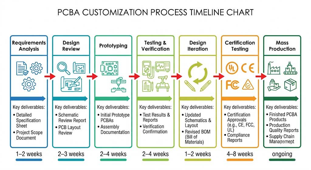
- Requirements Gathering (1-2 weeks): Define specifications, performance requirements, environmental constraints, and volume expectations
- Design Review (2-3 weeks): DFM analysis, schematic review, component selection, thermal analysis
- Prototyping (2-4 weeks): PCB fabrication, component sourcing, assembly, first article inspection
- Testing and Validation (2-4 weeks): Functional testing, environmental testing, EMC pre-compliance
- Design Iteration (1-2 weeks): Incorporate feedback, design modifications
- Certification (4-8 weeks): FCC, CE, IC certification testing
- Mass Production (ongoing): Volume manufacturing, quality control, shipping
| Phase | Duration | Deliverables |
|---|---|---|
| Requirements | 1-2 weeks | Requirements document, BOM draft |
| Design | 2-3 weeks | Gerber files, finalized BOM |
| Prototyping | 2-4 weeks | Prototype PCBs, test reports |
| Testing | 2-4 weeks | Test reports, validation data |
| Certification | 4-8 weeks | Certification documents |
| Production | Ongoing | Finished products |
During the Requirements Gathering phase, the design team works with the customer to develop a detailed product requirements document (PRD) that captures all technical specifications, environmental constraints, and commercial objectives. Key deliverables include: target RF performance metrics (output power, sensitivity, throughput), operating temperature range and enclosure requirements, power supply specifications (PoE voltage, maximum power consumption), interface requirements (Ethernet ports, GPIOs, serial interfaces), and certification requirements by target market. This phase typically involves 2-3 collaborative sessions between the customer’s engineering team and Zukaka’s design team, with the PRD serving as the contract between both parties for the remainder of the project.
The Design Review phase transforms the requirements into an electronic design. The schematic design captures all circuit details, the PCBA layout translates the schematic into a physical board design, and the DFM analysis reviews the layout for manufacturability. A formal design review meeting is held at the end of this phase, typically involving the customer’s engineering team, Zukaka’s RF engineers, and the manufacturing team. The review covers: RF signal chain analysis with link budget calculations; power supply design verification with worst-case current analysis; thermal simulation results showing junction temperatures across the operating range; component selection rationale with documented alternate sources; and test plan for the upcoming validation phase. The review gate at this point is critical — any design issues found at review should be resolved before proceeding to prototyping.
During Certification, the prototype boards undergo formal testing at accredited laboratories for the target markets’ regulatory requirements. FCC Part 15 testing in the US covers both intentional emissions (the WiFi transmitter) and unintentional emissions (spurious radiation from the digital circuits). CE RED testing in the EU adds requirements for radio performance and receiver immunity. The certification process is the most schedule-risky phase because test laboratory availability and test result interpretation can introduce delays. A well-prepared test campaign with pre-compliance data from the testing and validation phase can significantly reduce certification risk. For a wireless bridge PCBA, certification testing typically costs $15,000-30,000 per market and takes 4-8 weeks from test booking to certificate issuance.
Supplier Selection Checklist for Industrial PCBA
The supplier selection decision has a greater impact on your product’s quality, cost, and time-to-market than any other decision in the PCBA development process. A well-qualified supplier becomes a strategic partner who contributes engineering expertise during the design phase, provides cost optimization suggestions based on manufacturing experience, and delivers consistent quality across production runs. A poorly chosen supplier causes design re-spins, production delays, quality issues, and certification failures that can delay product launch by 6-12 months and add $50,000-200,000 in unexpected costs.
The evaluation criteria below are organized by priority, reflecting the specific requirements of industrial wireless PCBA rather than general electronics manufacturing. Each criterion includes the specific qualification evidence you should request from potential suppliers during the evaluation process.
- Quality certifications: ISO 9001:2015 certification (current, not expired) and documented IPC-A-610 Class 3 training for all assembly and inspection personnel. Request recent certification audit reports to verify that the certification is actively maintained rather than a certificate obtained years ago.
- Industrial wireless experience: Minimum 5 years of PCBA production for industrial wireless products, with specific experience in RF board assembly, high-frequency laminate materials, and high-reliability soldering processes. Request case studies of similar projects and contact information for 3-5 current clients.
- RF design and testing capability: In-house RF engineering team with experience in wireless chipset reference design implementation, RF impedance matching, antenna integration, and spectrum analysis. Verify that the supplier has RF test equipment (spectrum analyzers, network analyzers, signal generators) and personnel trained to use them.
- Production scalability: Demonstrated ability to transition from prototype (5-50 units) through pilot run (50-500 units) to mass production (500-10,000+ units) without requalification. The same processes and equipment should be used at all volumes — a supplier that uses different processes for prototyping vs. production introduces risk of yield changes at scale.
- Testing infrastructure: In-house ICT and FCT capabilities with documented test coverage targets. For wireless products, the FCT system should include a shielded RF test chamber and calibrated reference device for throughput and sensitivity measurements.
- Component supply chain management: Established relationships with authorized distributors for major semiconductor brands, documented alternate component qualification process, and proactive obsolescence monitoring system. Request lead time data for recent orders to assess real supply chain performance.
- Certification support experience: Previous experience with FCC, CE, IC, and other regulatory certifications for wireless products. The supplier should be able to provide pre-compliance testing data and work with accredited test laboratories to resolve issues during formal certification.
- Engineering communication: Responsive engineering support with a single point of contact for technical issues. English-language documentation and communication capability, with design review meetings available on a regular schedule during the development phase.
- Manufacturing lead times: Competitive turnaround times for both prototypes (2-4 weeks) and production (4-8 weeks for 1,000-10,000 units). Request current lead time data and on-time delivery statistics for recent orders.
- Customer references: Positive testimonials from current customers in similar industries, with permission to contact them for detailed discussions about their experience. A supplier’s existing customer base is a strong indicator of their capability and reliability.
Case Studies
Case Study 1: Industrial Wireless Bridge Manufacturer — Oil Field Deployment
The challenge was to develop a wireless bridge PCBA capable of reliable operation in oil field environments where temperatures range from -40°C to +85°C and the radio spectrum is congested with other oil field communication systems. The customer’s previous supplier had delivered boards that failed in the field after 6-12 months due to solder joint cracking from thermal cycling and RF interference from nearby radar systems. The customer needed a complete redesign with industrial-grade components, DFS support for radar avoidance, and a quality system that ensured consistent reliability across production runs.
Zukaka’s solution addressed all three failure modes through a comprehensive PCBA customization approach. The design used a Qualcomm-based chipset with integrated DFS firmware that automatically detects radar signals on the current channel and initiates a channel switch within 10 seconds, meeting FCC requirements for 5 GHz band operation. All 480 components on the board were selected with -40°C to +85°C temperature ratings, including industrial-grade MLCC capacitors with X7R dielectric that maintain stable capacitance across the temperature range. The assembly process was qualified to IPC-A-610 Class 3 standards, with 100% AOI inspection and temperature cycling screening applied to every production board.
Results: The redesigned PCBA achieved 99.9% field reliability over 18 months of deployment across 200+ oil field sites. The customer reported zero field failures attributable to the PCBA, compared to the 8% annual failure rate experienced with the previous supplier’s boards. The cost per board was reduced by 25% compared to the previous supplier through strategic component sourcing and DFM optimization, and the product passed FCC certification on the first testing attempt — a significant achievement given the complexity of DFS testing.
Case Study 2: IoT Sensor Company — Ultra-Low-Power Wireless Node
The challenge was to develop a miniaturized wireless sensor node PCBA with battery life exceeding 5 years on a single 18650 lithium cell, while maintaining reliable WiFi connectivity for data upload. The customer’s initial design consumed 350 mW in active mode and 50 mW in sleep mode, yielding an estimated battery life of only 8 months under typical operating conditions. The target was 5+ years, requiring an order-of-magnitude improvement in power efficiency. Additionally, the existing PCBA measured 85 mm x 55 mm — too large for the target 60 mm x 40 mm enclosure specified by the customer’s industrial design.
Zukaka’s solution involved a complete power architecture redesign and custom firmware optimization. The 6-layer PCBA used a low-leakage 4-layer stackup with dedicated power and ground planes that reduced power supply noise and allowed lower-voltage operation of the digital logic. The custom firmware implemented a duty-cycled operating scheme: the WiFi radio remains in deep sleep (5 µW) for configurable intervals (typically 5-15 minutes), wakes up in 8 ms, transmits sensor data in 150-300 ms, and returns to sleep. The average power consumption was reduced from 350 mW to 8 mW, a 44x improvement, while maintaining the same data transmission capability.
Results: The redesigned PCBA achieved a 4-layer compact layout measuring 58 mm x 38 mm — a 53% reduction in board area. The 8 mW average power consumption enables 5+ years of operation from a standard 3.7V 3500 mAh 18650 cell, assuming one data upload per 10 minutes. The per-board cost was reduced by 20% compared to the original design through elimination of unneeded components and consolidation of the power management ICs. The product achieved FCC and CE certification on the first submission.
PCBA Product Showcase — Customizable Industrial Wireless Motherboards
These four PCBA platforms represent the foundation for building industrial wireless products across the most common application categories. Each platform has been designed with modular customization in mind — the core RF and processing architecture remains fixed while the peripheral interfaces, power management, and mechanical configuration can be adapted to specific requirements. This approach reduces development time by 6-10 weeks compared to a ground-up design, while still delivering a product that is purpose-built for the target application.
| Product | Customization Options | Industrial Applications |
|---|---|---|
| 11ac 48V Long-Range Bridge PCBA | Temperature range (-40°C to +85°C), 48V/24V PoE, antenna options | Oil & gas, mining, power utilities, outdoor surveillance |
| 11ac 24V Gigabit Bridge PCBA | IP rating (IP65/IP67), power input, interface customization | Factory automation, warehouse logistics, industrial IoT |
| 2.4G Wireless Mesh Motherboard (YN300A) | Custom firmware, MANET protocol tuning, enclosure design | Emergency communications, underground mining, defense |
| 5GHz High-Power WiFi Module | Connector types, RF power, temperature grading | Wireless AP, routers, gateways, embedded systems |
The 11ac 48V Long-Range Bridge PCBA is the highest-performance platform, designed for backbone links and long-distance point-to-point connections. Its 48V PoE input supports cable runs up to 100 meters with standard Cat5e, and the high-efficiency DC-DC converter maintains stable operation even when the input voltage drops to 36V at the end of long cable runs. The board supports external antennas with N-type connectors, enabling the use of high-gain directional antennas for links up to 30 km. Typical customization requirements for this platform include: selecting the operating frequency band (5 GHz only or dual-band 2.4/5 GHz), configuring the Ethernet port count (1-2 ports with or without PoE passthrough), and tuning the RF output power to meet specific regulatory limits for different target markets.
The 2.4G Wireless Mesh Motherboard (YN300A) is purpose-built for mobile ad-hoc network (MANET) applications where traditional infrastructure-based networking is not feasible. Its firmware implements a proprietary mesh routing protocol that supports self-forming, self-healing network topologies with up to 50 nodes. Each node automatically discovers neighboring nodes, calculates optimal routing paths, and adapts to topology changes as nodes move or fail. The YN300A is commonly customized with: military-grade encryption (AES-256) for defense applications, specialized connector configurations for vehicle mounting, and extended battery management firmware for solar-powered deployments in remote areas.
Frequently Asked Questions About Industrial Wireless PCBA Customization
Q: What is the minimum order quantity for PCBA customization?
Zukaka accepts orders starting from 1 piece for prototyping and recommends a minimum of 100 units for production pricing. Prototype orders (1-10 units) are manufactured using the same processes and equipment as production orders, ensuring that prototype results are representative of production quality. Pilot run orders (50-500 units) are recommended for initial field deployments and certification testing, providing volume pricing while allowing any final adjustments before full production. For production orders above 500 units, we provide tiered pricing that decreases by 10-20% at each volume threshold, with the best pricing available at 5,000+ units per order.
Q: How long does PCBA customization take from concept to production?
The typical timeline for a new industrial wireless PCBA design is 8-16 weeks from initial requirements to production-ready design, depending on complexity and certification requirements. A simple derivative design — modifying an existing PCBA with different connectors, power input, or enclosure mounting — can be completed in 6-10 weeks. A ground-up design with new chipset, multi-layer board, and full certification testing typically requires 14-20 weeks. The critical path is almost always certification testing, which depends on external laboratory availability and can add 4-8 weeks to the schedule. We recommend discussing certification timelines early and booking test laboratory time during the design phase to minimize schedule impact.
Q: Can you help with firmware development for wireless PCBA?
Yes, Zukaka maintains a dedicated firmware engineering team with experience developing custom firmware for Qualcomm, MediaTek, Realtek, and other wireless chipsets. Our firmware development capabilities span the full spectrum from low-level driver development through operating system integration to application-layer software. We support Linux (kernel 4.x through 6.x), OpenWrt (21.x and 23.x), and custom RTOS implementations for resource-constrained designs. Typical firmware customization projects include: web-based management interface with NMS/SNMP support; custom QoS algorithms for video or voice prioritization; proprietary TDMA protocols for deterministic latency; secure boot implementation with signed firmware images; and cloud platform integration for remote device management.
Q: What quality standards do you follow for industrial PCBA?
Zukaka adheres to IPC-A-610 Class 3 standards for all industrial wireless PCBA production and maintains ISO 9001:2015 quality management certification. Class 3 compliance covers all aspects of assembly: solder joint acceptance criteria, component placement accuracy, board cleanliness, and mechanical integrity. Our manufacturing facility uses automated optical inspection (AOI) for 100% solder joint verification, in-circuit testing (ICT) for component-level electrical verification, and functional testing (FCT) for system-level performance verification. Environmental stress screening (temperature cycling, vibration testing) is available for applications requiring the highest reliability levels, such as oil and gas, defense, and critical infrastructure deployments.
Q: How do you handle component supply chain issues?
We maintain a formal component engineering process that identifies and qualifies at least two approved alternate components for every critical part on the BOM. This multi-sourcing strategy was developed in response to the 2021-2023 semiconductor shortages, which demonstrated that single-source dependency can halt production for 6-12 months when a component goes on allocation. Our supply chain management team monitors component lead times, end-of-life notifications, and market availability, providing proactive recommendations when components show signs of supply risk. For wireless chipsets specifically, we maintain strategic inventory of high-volume components and have long-term supply agreements with authorized distributors that guarantee priority allocation for our production orders.
Q: Can you assist with FCC/CE certification?
Yes, Zukaka provides full certification support from pre-compliance testing through formal certification at accredited laboratories. Our pre-compliance testing includes: conducted and radiated emission measurements using our in-house EMI test receiver and RF anechoic chamber; RF parametric testing (output power, frequency accuracy, modulation quality, spurious emissions); and ESD and surge immunity testing per IEC 61000-4. Pre-compliance testing is performed during the design validation phase, allowing us to identify and resolve issues before the formal certification campaign begins. For formal certification, we work with accredited test laboratories in the US (FCC), EU (CE RED), Canada (IC RSS-210), and other markets, managing the entire process from test plan development to certificate submission.
Q: What is your typical lead time for mass production?
For production orders of 1,000-10,000 units, our standard lead time is 4-6 weeks from order confirmation and BOM finalization. Lead time is driven primarily by component procurement (2-4 weeks for standard parts, 12-20 weeks for wireless chipsets) and PCBA fabrication (1-2 weeks). For orders requiring expedited delivery, we offer a 2-3 week expedited service at a 10-15% premium, subject to component availability. We recommend placing forecast orders 8-12 weeks in advance of required delivery to secure component allocation and avoid expedite charges. For ongoing production programs, we offer consignment inventory programs where we hold finished goods at our facility and ship against weekly release orders with a 1-2 week lead time.
Q: Do you provide after-sales support for custom PCBA?
Yes, Zukaka provides comprehensive after-sales support covering technical assistance, warranty service, and product lifecycle management. Technical support is available through our engineering team during business hours (UTC+8), with a target response time of 4 hours for critical issues and 24 hours for standard inquiries. All PCBA products carry a 12-month warranty against manufacturing defects, with warranty period options up to 36 months available for industrial customers with extended reliability requirements. Our product lifecycle management service includes: component obsolescence monitoring with 6-12 month advance notification; last-time-buy management for discontinued components; and redesign support to substitute obsolete components with current equivalents while maintaining form, fit, and function compatibility.
By: Zukaka Engineering Team |
Last Updated: June 14, 2026 |
Connect on LinkedIn
⭐⭐⭐⭐⭐ OEM/ODM Partner
“Zukaka PCBA modules have been integral to our industrial wireless product line. The engineering team’s responsiveness and the modules’ reliability in harsh environments have made them our preferred supplier for three consecutive years.”
— VP of Engineering, Industrial Wireless Equipment Manufacturer
⭐⭐⭐⭐⭐ System Integrator
“We’ve integrated Zukaka wireless bridge PCBA into our smart city and industrial IoT deployments. The industrial temperature range and long-range capabilities have consistently exceeded our specifications.”
— Technical Director, Systems Integration Company
✔ Certifications: FCC, CE, RoHS compliant |
✔ Industrial temperature range -40 to +85 °C |
✔ IP65-rated for outdoor deployment
Contact our engineering team for customized PCBA solutions and technical support.


