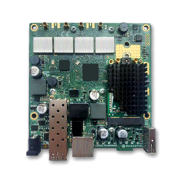
Detailed explanation of the complete production process of PCBA circuit boards
.tw-product { max-width: 1200px; margin: 0 auto; font-family: 'Segoe UI', Roboto, Arial, sans-serif; color: #1a1a2e; line-height: 1.8; font-size: 16px; padding: 0; background: #ffffff; } .tw-product h1 { font-size: 30px; font-weight: 800; color...
Complete PCB Manufacturing Process: From Gerber Review to Finished Goods Shipment
Product Overview
The PCB (Printed Circuit Board) serves as the “backbone” and “nerve center” of electronic devices, providing the foundation for component interconnection. Its manufacturing integrates precision mechanics, chemical processing, and electrical testing. Precision in every step directly affects performance and reliability. Based on actual production in professional PCB factories, this article explains the full PCB manufacturing flow from raw material to finished product.
Key Overview
Target Users:Electronics engineers, PCB designers, manufacturing professionals, quality control personnel
Core Strengths:Comprehensive process coverage, practical factory insights, step-by-step technical details
Typical Applications:PCB production guidance, quality control training, engineering reference
Technical Areas:Photolithography, electroplating, soldermask, testing
Quality Standards:IEC 61189, IPC-A-600
1. Pre-Production: File Review & Film Preparation
The first step in PCB manufacturing is Gerber file review and processing. Gerber files contain all critical design data: tracks, pads, vias, silkscreen, and more. Engineers verify line spacing, via size, copper thickness, and customer requirements (surface finish, material, board thickness) to ensure design compatibility with production capabilities.
After approval, phototools (films) are produced. These act as the “negative templates” for exposure and development, including circuit film, solder mask film, and silkscreen film. Film precision directly determines PCB accuracy and clarity.
Meanwhile, the workshop prepares raw materials. The core PCB substrate is copper-clad laminate (CCL), composed of insulation and copper foil. Common materials include FR-4 (general purpose), FR-1 (paper-based, low cost), and metal-core CCL (for high heat dissipation). Standard copper weights are 1oz, 0.5oz, and 2oz, selected based on current requirements.
2. Core Process: Circuit Pattern Transfer
Circuit fabrication is the core step, transferring the pattern from film to copper foil, also known as pattern transfer. The main steps are:
- Surface Cleaning & Buffing: Panels are cut to size, then brushed to remove oxides, oil, and contaminants, improving adhesion. Panels are washed and dried thoroughly.
- Dry Film Lamination: UV-sensitive dry film is laminated onto the clean copper surface using heat and pressure, ensuring no bubbles or wrinkles.
- Exposure: The board and film are aligned precisely and exposed to UV light. UV passes through transparent areas and cures the film; opaque areas remain uncured.
- Development: Uncured dry film is dissolved in developer solution, leaving a cured protective pattern matching the film.
- Etching: Unprotected copper is etched away using chemical solution, leaving only the desired circuit. Time, concentration, and temperature are tightly controlled to avoid under-etch or over-etch.
- Stripping: The remaining cured dry film is removed, revealing the finished circuit pattern.
3. Drilling & Desmear / PTH: Via Formation
Vias connect layers on a PCB, including through-hole, blind, and buried vias (common in HDI). Quality directly affects interlayer connection reliability. The process includes drilling and plating through-hole (PTH):
- CNC Drilling: High-precision CNC drills create holes per Gerber data. Bits range from 0.2mm for microvias to several mm for mounting holes. Debris is removed by air and coolant.
- Desmear & Electroless Copper Plating: Holes are desmeared and roughened. A thin layer of copper is chemically deposited on the insulating hole wall to create conductivity between layers, typically 0.3–0.5μm thick, free of voids or pinholes.
4. Electroplating: Enhance Conductivity
The thin electroless copper layer is insufficient for current-carrying requirements. electroplating thickens the copper. High-end PCBs may also include nickel and gold plating:
- Panel Plating: The board is placed in an electrolytic bath to plate copper uniformly over all traces and vias to the required thickness (e.g., ~35μm for 1oz).
- Pattern Plating (Optional): For high-precision boards, tin is plated as a mask before etching, allowing better control of trace thickness and spacing.
- Gold / Nickel Plating (Optional): Improves wear resistance, oxidation resistance, and conductivity for connectors and high-reliability applications. Other finishes include tin, silver, and OSP.
5. Solder Mask Application: Protect Circuits & Prevent Short Circuits
Solder mask is the insulating coating (green, red, blue, black, white) that protects circuits from oxidation and moisture and prevents solder bridging. Steps include:
- Pre-Treatment: The board is cleaned and buffed to remove contaminants and improve ink adhesion.
- Solder Mask Printing: Liquid solder mask is applied evenly over the board, except over pads and vias.
- Pre-Bake & Exposure: The ink is pre-dried, then exposed and cured through the solder mask film.
- Development: Uncured ink is removed, exposing solder pads and vias.
- Curing: The board is baked at high temperature to fully cure the solder mask for maximum insulation, durability, and thermal resistance.
6. Silkscreen: Markings & Labels
Silkscreen provides text, symbols, and logos for component assembly, testing, and repair, such as R1, C2, U1, polarity marks, logos, and part numbers.
Silkscreen ink is printed through a screen stencil and cured at high temperature to ensure clarity and durability. Text must be legible and must not cover pads or vias.
7. Profiling: Cut to Final Dimensions
After processing, panels are cut into individual PCBs. Common methods include:
- CNC Routing: Uses a CNC mill to create precise shapes, slots, and rounded corners for complex or irregular boards.
- Punching: Uses a die for high-volume, standard rectangular boards, offering high efficiency and low cost. After profiling, edges are deburred to remove sharp edges and prevent shorts.
8. Electrical Test: Ensure Performance
Electrical testing is critical before shipment, checking for open circuits, short circuits, faulty vias, and continuity failures.
- Flying Probe Test: High-speed movable probes test continuity and isolation. Ideal for small batches, prototypes, and irregular boards; no fixture needed.
- Bed of Nails Test: Uses a custom fixture with fixed probes for simultaneous testing. Extremely fast for mass production.
Failed boards are marked and reworked; good boards proceed to final surface finish and inspection.
9. Surface Finish: Improve Solderability & Oxidation Resistance
Surface finish protects exposed copper from oxidation and improves solderability. Common types:
| Surface Finish | Key Characteristics | Applications |
|---|---|---|
| OSP | Thin, eco-friendly, low-cost protective layer | Consumer electronics, general applications |
| Tin Plating | Good oxidation resistance and solderability, medium cost | Industrial electronics |
| ENIG / Gold Plating | Nickel-gold layer with excellent conductivity, oxidation resistance, and reliability | Military, aerospace, high-end devices |
| Silver Plating | High conductivity | High-frequency communication boards |
| ENEPIG | Nickel-Palladium-Gold | HDI and flexible PCBs |
After surface finishing, boards are cleaned to remove chemical residues.
10. Final Inspection & Packaging
- Final Visual Inspection: Inspectors check for scratches, bubbles, pinholes, clear silkscreen, burrs, dimensions, thickness, warpage, and appearance.
- Packaging: Approved boards are packed in anti-static bags, vacuum-sealed, or separated with cardboard to prevent ESD damage, scratches, and moisture. Labels show model, quantity, date, and batch.
- Shipment: Finished PCBs are delivered per customer requirements, completing the full manufacturing process.
11. Key PCB Manufacturing Guidelines
Precision Control
Trace spacing, via size, and hole position require micron-level accuracy. Strict control of temperature, concentration, and time is essential throughout all processes.
Cleanliness
Dust-free, ESD-safe environments are required. Contamination causes defects in imaging, plating, and soldermask applications.
Environmental Compliance
Wastewater treatment and eco-friendly chemicals are mandatory to meet environmental regulations and sustainability standards.
Quality System
Full traceability and inspection records from incoming materials to finished goods ensure consistent quality and compliance.
Summary
PCB manufacturing is a precision, complex, multi-stage process involving mechanical processing, chemistry, electrical testing, and alignment. Attention to detail in every step ensures high-quality boards.
As electronics become smaller, more precise, and more reliable, PCB technology advances with HDI, flexible, and rigid-flex PCBs. Professional manufacturers continuously upgrade equipment, optimize processes, and strengthen quality control to provide high-performance PCBs for global industries, supporting the development of the entire electronics supply chain.
Frequently Asked Questions
Q: What is the typical lead time for PCB production?
Lead time varies by complexity and quantity. Standard FR-4 boards typically take 3-7 days for small batches, while high-layer-count HDI boards can take 10-14 days or longer.
Q: What file formats are required for PCB manufacturing?
Gerber RS-274X files are standard, along with drill files (Excellon format). Additional files like ODB++ or IPC-2581 may be required for advanced manufacturing.
Q: How to choose the right surface finish?
OSP is cost-effective for most consumer electronics. ENIG is recommended for high-reliability applications, connectors, or when multiple reflow cycles are needed. Tin is a good balance between cost and performance.
Q: What is the minimum via size and trace width?
Standard PCBs can handle 0.3mm vias and 0.1mm traces. Advanced processes can achieve 0.1mm vias and 0.05mm traces for HDI applications.


