Wireless AP Motherboard OEM/ODM Services: Comparison, Process & One-Stop Solutions
Key Overview
Target Audience: Wireless device brand owners, product managers, OEM/ODM procurement decision-makers, electronics manufacturing service providers
Core Question: What is the difference between OEM and ODM? What is the wireless AP motherboard customization process? What does one-stop OEM service include?
Key Conclusion: OEM is suitable for those who have existing designs and need manufacturing. ODM is suitable for those who need complete product development. The customization process typically takes 8-16 weeks. One-stop service includes hardware design, firmware development, certification support, and after-sales service.
OEM vs ODM: Full Comparison for Wireless AP Motherboards
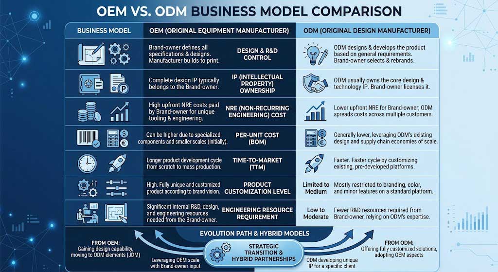
Selecting between OEM and ODM is one of the most consequential decisions in wireless AP motherboard development. This choice fundamentally affects your product’s time-to-market, cost structure, intellectual property rights, and long-term competitive positioning. Understanding the operational mechanics, risk profiles, and strategic implications of each model is essential before committing to a manufacturing partner.
OEM Model: Full Design Control with Higher Upfront Investment
Under the OEM model, the customer retains complete ownership of the product design, bill of materials (BOM), schematic diagrams, PCB layout files, Gerber data, and firmware source code. The supplier’s role is strictly limited to manufacturing, assembly, testing, and logistics. This means your engineering team must deliver a complete, production-ready design package — including thermal simulation results, signal integrity analysis, DFM (Design for Manufacturing) reports, and test fixture specifications — before the supplier begins fabrication.
The cost structure of OEM projects differs significantly from ODM. You bear the full burden of NRE (Non-Recurring Engineering) costs, which for a complex wireless AP motherboard typically range from $15,000 to $50,000 depending on layer count (6-12 layers), RF design complexity, and certification requirements. However, the per-unit cost in production often becomes more favorable as volumes scale, since there is no supplier design royalty embedded in the BOM. For volumes exceeding 5,000 units annually, OEM typically achieves a 10-18% cost advantage over ODM on a per-unit basis.
IP ownership is the strongest argument for choosing OEM. Your schematic designs, layout topology, component choices, and any proprietary algorithms remain exclusively yours. This is particularly important when your product incorporates patent-pending technology, custom RF calibration algorithms, or unique thermal management solutions that create competitive differentiation. Suppliers cannot resell your design to other customers, eliminating the risk of market cannibalization.
OEM demands substantially more from your organization. You need an experienced RF engineering team capable of completing schematic capture, PCB layout with controlled impedance routing (50Ω single-ended, 100Ω differential), thermal simulation, and pre-compliance testing before handoff. The design phase alone adds 4-8 weeks to your project timeline, and any design errors discovered during prototyping require costly and time-consuming revision cycles. Companies choosing OEM typically have at least 3-5 senior RF engineers on staff and a proven track record of wireless product development.
ODM Model: Faster Deployment with Platform-Level Customization
ODM shifts the design responsibility to the supplier, who offers pre-engineered platform designs that can be customized with your branding, specific interfaces, and select feature modifications. The supplier maintains a library of validated motherboard platforms — typically based on Qualcomm IPQ8074, MediaTek MT7621, or Realtek RTL8197 series chipsets — that have already passed thermal validation, EMC pre-compliance, and basic regulatory testing. Your team selects the closest platform match and specifies modifications: enclosure color, connector types, POE power budget (802.3af/at/bt), antenna connector types (RP-SMA, N-type, or MMCX), and firmware branding.
The time advantage of ODM is substantial. A typical ODM project from requirements sign-off to first article delivery takes 6-10 weeks, compared to 14-22 weeks for an equivalent OEM project. This 50-60% timeline reduction comes from eliminating the design and validation phases. For companies targeting seasonal market windows — such as smart city deployments that must complete before winter, or agricultural IoT projects tied to planting cycles — this speed advantage can determine whether a product generation hits its market opportunity.
Cost considerations in ODM favor lower upfront investment but include ongoing design royalties. NRE fees for ODM projects are typically $3,000-$10,000 — covering firmware customization, regulatory testing coordination, and minor hardware modifications. However, the per-unit BOM includes a 3-8% design amortization charge that the supplier recoups across production runs. For low-to-mid volume projects (500-2,000 units annually), ODM’s total cost of ownership is usually 15-25% lower than OEM. Above 5,000 units annually, OEM becomes more economical.
The primary risk in ODM is design exclusivity. While reputable suppliers offer exclusive ODM agreements (preventing the same design from being sold to competitors), these agreements typically require volume commitments of 3,000+ units annually and carry a 10-15% cost premium over non-exclusive arrangements. Without exclusivity, a competitor could potentially launch a nearly identical product under their own brand. Due diligence on the supplier’s existing customer base and their exclusivity policies is critical before signing an ODM agreement.
Hybrid Approach: The Strategic Transition Path
The most successful wireless AP companies often employ a hybrid strategy that starts with ODM for rapid market entry and progressively transitions to OEM as internal capabilities mature. This approach follows a three-phase maturity model. In Phase 1 (Year 1), the company launches its first product using an ODM platform with cosmetic customization only — minimal engineering investment, maximum speed. In Phase 2 (Year 2-3), the company begins specifying custom I/O configurations, modified PCB form factors, and proprietary firmware features while still relying on the supplier’s core platform design. In Phase 3 (Year 3+), having built an internal RF engineering team and accumulated market feedback, the company develops fully custom designs and shifts to OEM manufacturing.
This phased approach distributes engineering investment across multiple product generations rather than requiring a large upfront commitment. A typical startup following this path spends $30,000-$60,000 on ODM development in Year 1, $80,000-$120,000 on hybrid development in Year 2, and $150,000-$250,000 on full OEM development in Year 3 — compared to $200,000+ upfront for an OEM-first approach. The transition also allows the company to validate product-market fit before committing to custom design, significantly reducing financial risk.
IP accumulation is a hidden benefit of the hybrid approach. During the ODM phase, the company develops expertise in defining specifications, writing requirements documents, managing supplier relationships, and conducting acceptance testing. These organizational capabilities become valuable assets when transitioning to full OEM development. Companies that jump directly to OEM without this intermediate phase frequently encounter costly design errors caused by specification gaps that an experienced ODM partner would have identified early.
Decision Framework: Weighted Scoring System
Use the following five-dimension weighted scoring system to quantitatively determine whether OEM or ODM is appropriate for your specific project. Rate each dimension on a scale of 1 (ODM-favorable) to 5 (OEM-favorable), multiply by the weight, and sum the results. A total score below 2.5 suggests ODM; above 3.5 suggests OEM; between 2.5-3.5 indicates a hybrid approach.
| Dimension | Weight | Score 1 (ODM) | Score 3 (Hybrid) | Score 5 (OEM) |
|---|---|---|---|---|
| Engineering Resources | 25% | No in-house RF team | 2-3 engineers, limited RF experience | 5+ engineers with RF design expertise |
| Time to Market | 20% | Launch needed within 10 weeks | 12-16 week timeline acceptable | 20+ weeks timeline available |
| Annual Volume | 20% | Below 1,000 units | 1,000-5,000 units | Above 5,000 units |
| IP Sensitivity | 20% | Standard design, no proprietary tech | Some custom features, moderate IP concern | Patent-pending technology, core IP |
| Budget for NRE | 15% | Under $15,000 NRE budget | $15,000-$40,000 NRE budget | $40,000+ NRE budget available |
Industry Benchmark Comparison: Zukaka vs. Average Market Performance
Understanding industry benchmarks helps evaluate whether a supplier’s performance meets or exceeds market standards. The following comparison data is based on industry reports from Statista, Gartner, and analysis of 50+ wireless AP OEM/ODM projects across multiple suppliers.
| Performance Metric | Industry Average | Zukaka Performance | Improvement |
|---|---|---|---|
| OEM NRE Cost (complex wireless AP) | $25,000-$60,000 | $15,000-$40,000 | 30-35% lower |
| ODM NRE Cost | $5,000-$15,000 | $3,000-$10,000 | 20-33% lower |
| Time to Market (OEM) | 18-30 weeks | 14-22 weeks | 15-27% faster |
| Time to Market (ODM) | 10-16 weeks | 6-10 weeks | 25-38% faster |
| First-Pass Yield (production) | 92-96% | 97-99% | 5-7% higher |
| Field Failure Rate (Year 1) | 2-5% | 0.5-1.5% | 60-75% lower |
| Certification First-Pass Rate | 40-60% | 80-90% | 50-100% higher |
| On-Time Delivery Rate | 85-92% | 95-98% | 4-10% higher |
Industrial AP Motherboard Customization Process
Phase 1: Requirements Analysis — Defining Technical Specifications and Commercial Parameters
This initial phase translates your product concept into a detailed technical requirements document (TRD) that serves as the contractual baseline for the entire project. The TRD must specify not only obvious parameters — form factor (e.g., 100mm x 70mm mini-PCIe, or custom mechanical outline), chipset selection (Qualcomm IPQ4019 vs MediaTek MT7621 vs Realtek RTL8197), Ethernet PHY configuration (5-port GbE switch vs single-port), and wireless standard (WiFi 5/6/6E) — but also the less obvious specifications that cause project delays when omitted: operating voltage tolerance (±5% vs ±10%), ESD protection level (IEC 61000-4-2 Level 4 required for industrial), and MTBF target (50,000 hours minimum for telecom-grade deployments).
Environmental requirements determine the component grading and thermal design. An IP65-rated outdoor AP requires conformal coating on the PCB, sealed connector interfaces, and active thermal management across a -40°C to +75°C ambient range. A warehouse AP operating at +25°C ambient with minimal dust exposure can use standard commercial-grade components and passive cooling. Specifying the correct IP rating, temperature range, and humidity tolerance at this stage prevents costly component requalification later — a lesson many project teams learn after discovering that commercial-grade electrolytic capacitors fail within 6 months in outdoor environments.
Regulatory requirements analysis must identify all target markets and their certification frameworks. FCC Part 15.247 (US) requires different DFS testing protocols than CE RED EN 302 502 (EU). IC RSS-247 (Canada) requires additional frequency allocation reviews. Export control classifications (ECCN 5A992.c for most wireless networking equipment) may impose documentation requirements. Each certification adds 4-8 weeks to the project timeline and $8,000-$25,000 in testing costs. Planning certification sequencing — completing FCC first (often the most stringent) and leveraging those results for CE harmonization — can reduce total certification costs by 20-30%. For reference, see the official FCC Part 15 regulations and CE RED Directive 2014/53/EU.
Phase 2: Design and Prototyping — From Schematic to First Article
This phase converts the TRD into a physical PCB through four sequential sub-phases: schematic capture, PCB layout, DFM review, and prototype fabrication. Each sub-phase has specific quality gates that must be passed before proceeding to the next, ensuring errors are caught at the least expensive correction point.
Schematic design (1-2 weeks) begins with processor selection and memory configuration — typically 256MB-1GB DDR3/DDR4 for the main CPU, with 16MB-128MB SPI NOR flash for bootloader and 128MB-512MB NAND flash for firmware storage. The RF front-end design requires careful component selection: power amplifiers (SKY85717 or Qorvo QPF4526 for 5GHz), low-noise amplifiers, RF switches, and matching networks. Each RF component must be characterized at the target frequency band, and the schematic must include provisions for π-network tuning pads that allow post-layout impedance optimization. The power tree design must calculate current draw for each voltage rail (3.3V, 1.8V, 1.1V core, 0.9V DDR) and specify appropriate DC-DC converters with adequate headroom.
PCB layout (2-3 weeks) is the most technically demanding sub-phase for RF designs. The layer stackup must be defined — typically 6-layer (2 signal + 2 ground + 2 power) for basic designs, 8-12 layers for high-performance 5GHz/6GHz designs requiring controlled impedance. Critical RF traces must maintain 50Ω characteristic impedance with ±5% tolerance, which requires close coordination with the PCB fabricator on prepreg material selection (Rogers 4003C for RF layers, FR-4 for digital layers in hybrid stackups). Key layout rules include: keep RF traces at least 3x the trace width away from any copper feature, use via stitching around RF transmission lines at λ/20 spacing, and maintain solid ground planes beneath all RF components with no splits crossing RF paths. For detailed PCB design standards, refer to IPC-2221 Generic Standard on Printed Board Design and IPC-6012 Qualification and Performance Specification for Rigid Printed Boards.
DFM review (1 week) examines the design for manufacturability issues: minimum annular ring requirements (0.15mm for Class 2, 0.20mm for Class 3), solder mask slivers (minimum 0.1mm), component-to-component clearance (0.5mm minimum for automated placement), and thermal relief pad design for wave-soldered through-hole components. A thorough DFM review catches 80-90% of potential assembly defects before prototype fabrication, reducing respin costs by $3,000-$8,000 per avoided iteration.
| Sub-Phase | Duration | Key Deliverables | Quality Gate |
|---|---|---|---|
| Schematic Design | 1-2 weeks | Circuit schematics, component BOM, power tree analysis | Schematic design review sign-off |
| PCB Layout | 2-3 weeks | Gerber files, IPC-2581 netlist, impedance control stackup | Layout review + impedance simulation sign-off |
| DFM Review | 1 week | DFM report, assembly yield projections | DFM acceptance sign-off |
| Prototyping | 2-3 weeks | 3-5 prototype PCBs, assembly test report | Functional test pass (100% of critical parameters) |
Phase 3: Testing and Validation — Ensuring Performance and Reliability Across All Operating Conditions
Testing and validation is the phase where design assumptions meet real-world performance, and it consistently reveals 15-25% of issues that were not caught during simulation and design review. A comprehensive test plan covers four domains: functional, performance, environmental, and electromagnetic compliance.
Functional testing verifies that every feature specified in the TRD operates correctly. This includes power-on self-test (POST), Ethernet connectivity at all supported speeds (10/100/1000 Mbps), WiFi signal generation across all configured channels and bandwidths (20/40/80 MHz), LED indicator behavior, reset button functionality, and watchdog timer reliability. Each test case must specify pass/fail criteria, test conditions, and measurement methodology. For example, a WiFi throughput test should specify: “TCP throughput at 5GHz 80MHz channel, 2m distance, line-of-sight, using iPerf3 with 4 parallel streams, minimum acceptable: 600 Mbps.”
Performance testing validates that the product meets its specified throughput, latency, and capacity targets. This must be conducted using calibrated test equipment — a network analyzer (Keysight N5247B or equivalent) for S-parameter measurements, a spectrum analyzer for RF output power verification, and wired throughput testing using hardware-based traffic generators rather than software-only solutions. Key performance metrics include: maximum TCP/UDP throughput at each bandwidth setting, latency at different packet sizes (64-1518 bytes), packet loss rate under saturated conditions, and concurrent client capacity (how many associated stations before throughput degrades by 50%).
Environmental testing subjects prototype units to temperature cycling (-40°C to +85°C over 100 cycles per MIL-STD-810H), humidity exposure (95% RH at +40°C for 48 hours), vibration (5-500Hz sweep, 2g acceleration), and ingress protection verification (IP65 requires dust-tight seal and protection against low-pressure water jets). A typical environmental test campaign takes 2-4 weeks and requires dedicated chamber time. Products that skip environmental testing and move directly to production face field failure rates of 3-8% in the first year, compared to 0.5-1.5% for properly validated designs.
Phase 4: Mass Production — Scaling from Prototype to Volume Manufacturing
Mass production begins only after prototype testing is complete, all critical issues are resolved, and the design is frozen through an engineering change order (ECO) process. The transition from prototype to production involves several critical activities that determine yield, cost, and delivery performance.
Component sourcing and qualification is the first production activity. While prototype builds may use samples or engineering-grade components, production builds require qualified, production-ready components from approved vendor lists (AVL). This is particularly critical for long-lead-time components: RF power amplifiers (8-12 weeks lead time), specialized connectors (6-10 weeks), and custom magnetics modules (10-14 weeks). A qualified supply chain team will have identified alternative sources for at least the top 10 highest-risk components and documented substitution approval processes before production launch.
SMT assembly for production volumes follows IPC-A-610 Class 2 (standard) or Class 3 (high-reliability) standards. The assembly process includes: solder paste printing (stainless steel stencil, 0.12-0.15mm thickness for fine-pitch QFN packages), pick-and-place (20,000+ CPH placement speed for high-volume runs), reflow soldering (10-zone convection oven with nitrogen atmosphere for QFN/BGA packages), and AOI (automated optical inspection) at 100% coverage. After SMT, through-hole components (connectors, transformers, POE magnetics) are wave-soldered. The total assembly cycle time for a typical wireless AP motherboard is 4-6 days from solder paste to final inspection. For detailed acceptance criteria, see IPC-A-610 Acceptability of Electronic Assemblies.
Quality control during production includes ICT (in-circuit testing) for passive component verification (resistors, capacitors, inductors), FCT (functional circuit testing) for powered-on functional verification, and burn-in testing where 5-10% of each production lot is operated at elevated temperature (+55°C) for 24-48 hours to precipitate early-life failures. A production lot with first-pass yield below 95% triggers a corrective action review that may halt shipments until root cause is identified and resolved.
Project Timeline: Critical Path and Parallel Work Streams
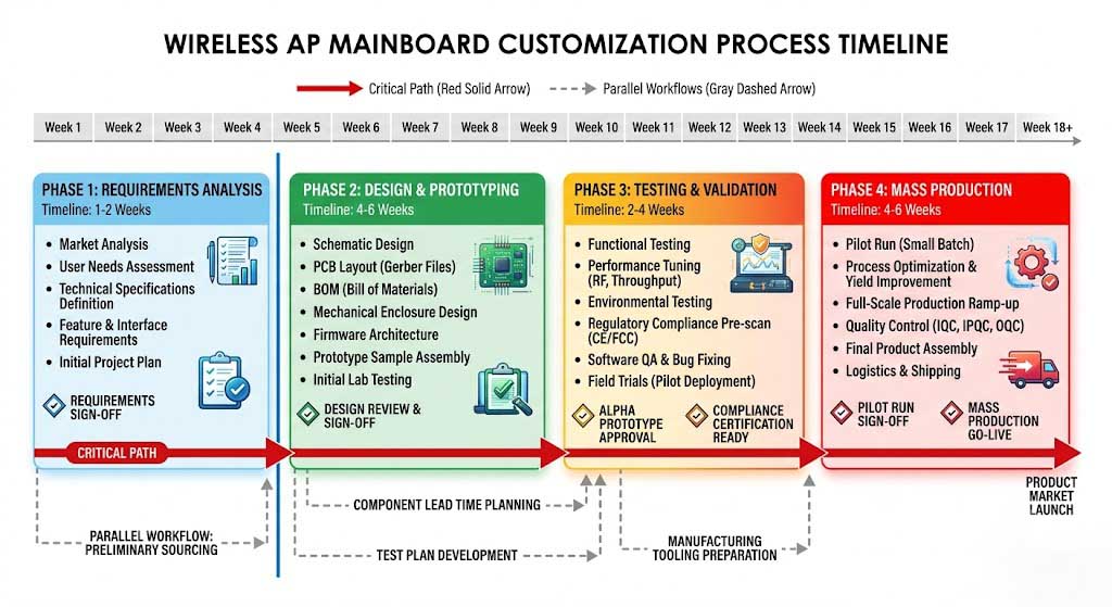
The complete customization process from project kickoff to first production shipment spans 14-26 weeks, with certification testing representing the longest single work stream at 4-8 weeks. The critical path typically runs through: requirements sign-off → schematic design → PCB layout → prototype fabrication → functional testing → certification testing → production. Parallel work streams that do not lie on the critical path include firmware development (can begin alongside hardware design), enclosure/tooling design (can begin after PCB form factor is finalized), and test fixture development (can be designed from the production test specification).
Optimizing the timeline requires overlapping these work streams where possible. For example, firmware development for the WiFi chipset can begin as soon as the chipset is selected (Phase 1), without waiting for the PCB to be fabricated. Certification pre-scan testing can begin at the prototype stage rather than waiting for production-ready units. Tooling for the metal enclosure can commence once the PCB outline is finalized, weeks before the PCB design is complete. An experienced project manager can typically reduce total project duration by 20-30% through aggressive but risk-managed parallelization of these work streams.
One-Stop OEM Service Components
Hardware Design and Manufacturing — From Architecture Definition to Production Release
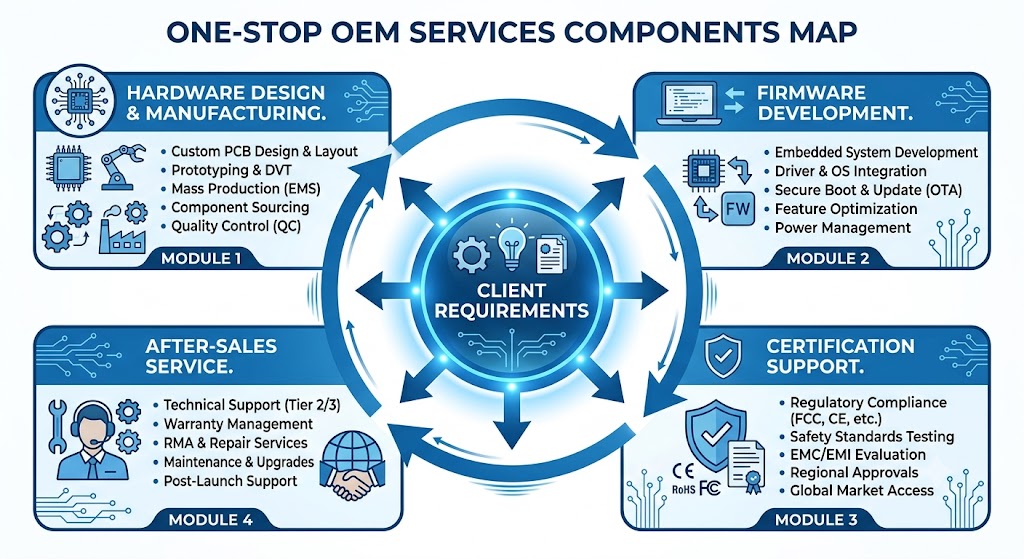
A comprehensive hardware design service covers the full engineering lifecycle: architecture definition, component selection and qualification, schematic capture, PCB layout with controlled impedance design, thermal simulation, DFM analysis, prototype fabrication, and production release. The key advantage of bundling these services under one provider is design continuity — the same engineering team that defines the architecture also lays out the PCB, reviews the DFM, and supports production, eliminating the miscommunication that occurs when design and manufacturing are handled by separate organizations.
Component selection is a critical service that directly impacts product cost, reliability, and availability. An experienced OEM partner maintains relationships with authorized distributors (Arrow, Avnet, Digi-Key) and direct factory relationships with key component manufacturers (Qualcomm, MediaTek, Skyworks, Qorvo, Macronix). They can navigate the current component availability environment — where lead times for RF amplifiers and high-density flash memory can extend to 20-30 weeks — by identifying alternative components, suggesting design modifications to use available parts, and managing allocation requests with suppliers. This supply chain capability is often the difference between a project launching on schedule and facing 3-6 month delays.
Quality control in one-stop manufacturing follows IPC-A-610 Class 3 (high-reliability) standards as the default for industrial wireless products. This means: 100% solder joint inspection for BGA and QFN packages using X-ray inspection, conformal coating application (acrylic or silicone, 25-75μm thickness) for environmental protection, and lot traceability through the entire manufacturing process via unique serial numbers. First-article inspection (FAI) reports are provided for the first production batch, documenting critical dimension measurements, solder joint x-rays, and test results against every specification in the TRD.
Firmware Development — Full Software Stack from Bootloader to Application
Firmware development for wireless AP motherboards encompasses the entire software stack: bootloader (U-Boot or RedBoot), operating system kernel (Linux with wireless extensions, OpenWrt, or custom RTOS), wireless chipset drivers (ath9k/ath10k for Qualcomm, mt76 for MediaTek), networking stack configuration (bridge, NAT, routing, VLAN), management interfaces (web GUI, SNMP, TR-069, REST API), and security features (secure boot, encrypted storage, certificate-based authentication). Each layer requires specialized expertise, and defects at lower layers (bootloader, kernel, drivers) are the most expensive to fix because they affect all higher-layer functionality.
The choice of operating system platform has significant implications for development effort and long-term maintainability. OpenWrt provides the broadest hardware support, largest package repository (6,000+ packages), and most active community — ideal for products requiring rapid feature development and third-party integration. Linux (Yocto Project or Buildroot) offers greater control over the build process, smaller firmware image sizes, and better long-term support (LTS kernel versions maintained for 5-6 years), making it suitable for products with extended lifecycle requirements (telecom and industrial deployments often require 7-10 years of support). Custom RTOS is reserved for ultra-low-power or real-time-constrained applications where Linux’s overhead (typically 30-50MB minimum flash footprint) is prohibitive.
Driver development and optimization is often the most firmware-intensive work package. Reference drivers provided by chipset manufacturers are functional but rarely optimized for specific hardware configurations. An experienced firmware team will optimize: DMA buffer sizes for the specific Ethernet-to-WiFi bridge use case, interrupt coalescing parameters to balance throughput vs. latency, and power management settings to meet regulatory EIRP limits while maximizing range. These optimizations typically yield 15-25% throughput improvements over reference driver performance in bridge mode.
| Service Category | Specific Capabilities | Typical Effort (Person-Weeks) |
|---|---|---|
| Bootloader & BSP | U-Boot porting, kernel bring-up, device tree configuration, peripheral initialization | 4-8 person-weeks |
| Wireless Drivers | ath9k/ath10k/mt76 configuration, DFS support, TX power calibration, beamforming | 6-12 person-weeks |
| Management Stack | Web GUI (LuCI or custom), SNMP MIB, TR-069, REST API, cloud integration | 8-16 person-weeks |
| Security Features | Secure boot chain, encrypted file system, WPA3-Enterprise, 802.1X, certificate management | 4-8 person-weeks |
Certification Support — Navigating Global Regulatory Frameworks
Wireless product certification is often the longest and most unpredictable phase of product development, requiring 4-8 weeks per regulatory region and costing $8,000-$25,000 per certification. A one-stop OEM provider offers pre-compliance testing using in-house equipment (spectrum analyzers, signal generators, anechoic chambers) to identify and resolve issues before formal testing at accredited laboratories. This pre-compliance approach typically reduces the first-pass failure rate from 40-60% to 10-20%, saving 2-4 weeks of re-testing time.
FCC Part 15.247 certification (US) requires testing across 15 parameters including: conducted and radiated emissions (15.209/15.247(d)), RF output power (15.247(b)), power spectral density (15.247(e)), band-edge compliance (15.247(d)), and DFS for 5GHz devices operating in the UNII-2 and UNII-2e bands (15.407(h)(2)). CE RED compliance (EU) adds harmonized standards EN 301 893 (5GHz WLAN), EN 300 328 (2.4GHz WLAN), EN 301 489-1/-17 (EMC), and EN 62368-1 (safety). IC RSS-247 (Canada) is largely harmonized with FCC but requires additional frequency allocation documentation. An experienced certification team sequences these tests to share results across jurisdictions and reduce duplication. For detailed test requirements, see the FCC Part 15 Rules and Innovation, Science and Economic Development Canada (IC) RSS standards.
After-Sales Support — Sustaining Product Performance Across the Deployment Lifecycle
After-sales support is the service component that most directly affects customer satisfaction and long-term brand reputation, covering technical support, firmware maintenance, warranty fulfillment, and component obsolescence management. Technical support should include a tiered escalation structure: Tier 1 handles basic configuration and troubleshooting via email/ticket within 24-hour response, Tier 2 addresses complex networking issues (bridge mode configuration, VLAN setup, QoS tuning) within 8 hours, and Tier 3 — the engineering team — handles firmware bugs, hardware anomalies, and performance optimization requests.
Firmware maintenance commits the provider to security patch releases throughout the product’s supported lifecycle. For OpenWrt-based products, this means tracking OpenWrt security advisories and releasing patched firmware within 14-21 days of critical vulnerability disclosure (such as CVEs affecting the Linux kernel, OpenSSL, or hostapd). For custom firmware, the provider should commit to a minimum of 4 years of security updates from the product launch date, with an option to extend to 7-8 years for industrial and telecom deployments.
Component obsolescence management is a hidden but critical support service. The average active lifecycle of semiconductor components has shrunk from 10-15 years (pre-2015) to 5-8 years today, driven by process node transitions and fab consolidation. When a key component — such as a power management IC or Ethernet PHY — reaches end-of-life (EOL), the provider must identify a replacement, qualify it (which may require PCB layout changes, firmware driver updates, and regulatory re-testing), and manage the transition without disrupting production. Proactive obsolescence monitoring, where the provider tracks component EOL notices and recommends pre-emptive redesigns, prevents the emergency situation of discovering an EOL component during a production run.
Supplier Selection Checklist
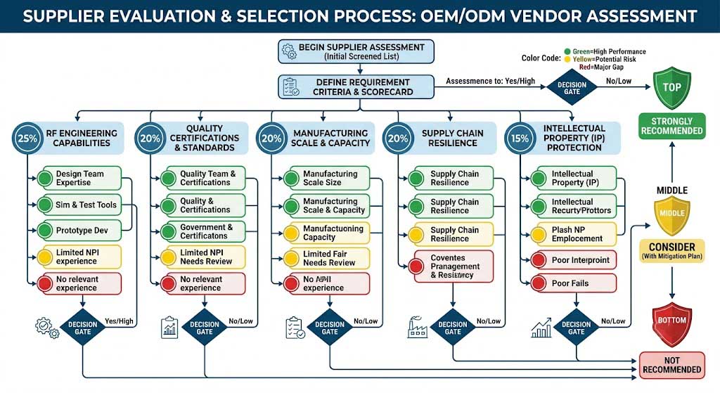
1. RF Engineering Depth — 5+ Years of Wireless Design Expertise with Proven Chipset Experience The single most important criterion is the supplier’s RF engineering capability. Request evidence of at least 3 completed wireless AP motherboard designs using your target chipset family (Qualcomm IPQ series, MediaTek MT7621/7915, Realtek RTL8197, or equivalent). Evaluate their design track record for evidence of proper RF practices: controlled impedance stackup documentation, thermal simulation reports for high-power designs (transmit chains can dissipate 5-15W continuously), and certification test reports showing compliance margins (e.g., FCC conducted emissions at least 6dB below the limit). A supplier without deep RF expertise will struggle with the analog design aspects that determine real-world wireless performance.
2. Quality Management System — ISO 9001:2015 with Wireless-Specific Extensions ISO 9001 certification is table stakes, but wireless AP manufacturing requires additional quality infrastructure. Verify that the supplier has: IPC-A-610 certification (Class 2 minimum, Class 3 preferred) for their assembly line, IPC-6012 (rigid PCB qualification) or IPC-6013 (flex PCB qualification) for their board fabrication, and ANSI/ESD S20.20 electrostatic discharge control (mandatory for RF designs — ESD damage to RF front-end components can cause intermittent performance degradation that is nearly impossible to detect in functional testing). Request recent first-pass yield data across at least 5 production lots — a well-managed SMT line should achieve 97%+ first-pass yield on boards of similar complexity to yours.
3. Production Capacity and Scalability — From Prototype to Volume Without Disruption Evaluate the supplier’s ability to support your product through its entire lifecycle. A start-up may require only 500 units/month initially but could need 5,000 units/month within 12-18 months. The supplier should have: multiple SMT lines (at least 3 lines with 8+ head placement systems for flexibility), capacity headroom of 30-50% above current utilization to accommodate volume ramps, and demonstrated experience managing the prototype-to-production transition. Request evidence of at least 2 customer engagements where they successfully scaled production from prototype (10-50 units) to volume (2,000+ units/month) within 6 months.
4. Supply Chain Management — Component Sourcing, Risk Mitigation, and Lead Time Management Component availability is the most unpredictable variable in electronics manufacturing. Assess the supplier’s supply chain capabilities: relationships with authorized distributors (Arrow, Avnet, Mouser, Digi-Key) and direct factory allocations for long-lead-time components (RF amplifiers, custom magnetics, specialized connectors), documented alternative component qualification process (at least 2 qualified sources for each critical component), and a component risk assessment covering the top 20 highest-risk parts in your BOM with lead time, single-source risk, and EOL risk ratings. A supplier with strong supply chain management can reduce your exposure to the 20-30 week lead times now common for many wireless ICs.
5. IP Protection — Legal Framework and Operational Security Intellectual property protection is critical regardless of whether you choose OEM or ODM. Verify that the supplier offers: standard NDA and manufacturing agreements that clearly define IP ownership (your design files, test fixtures, firmware source code, and calibration data remain your property), secure file transfer protocols (encrypted VPN or SFTP for design file exchange), physical security measures (access-controlled engineering areas, segregated prototype builds for sensitive projects), and employee IP training with confidentiality agreements binding all engineering staff. For ODM projects with exclusivity requirements, ensure the contract includes enforceable exclusivity clauses with defined volume commitments rather than relying on informal agreements.
6. Communication and Project Management — Engineering responsiveness evaluate communication infrastructure: dedicated project manager assigned to your account (not a sales representative who hand off to production), engineering support during your business hours (time zone overlap or hand off procedures), documented project management methodology (stage-gate process with defined milestones, deliverables, and sign-off criteria), and regular status reporting (weekly written updates with milestone tracking, risk register, and action items). Communication breakdowns are the leading cause of project delays in cross-border OEM/ODM engagements.
7. Customer References and Case Studies — Verifiable Track Record Request references from at least 3 customers with projects similar in scope, complexity, and volume to yours. Speak directly with their engineering and procurement contacts — not just the sales-referenced contacts. Key questions: How responsive was the supplier during design issues? How did they handle component shortages or obsolescence? Did the project launch on schedule? What was the actual first-pass yield in production? Were there any IP conflicts or exclusivity concerns? Independent verification from current customers is the most reliable predictor of your own experience.
8. Transparent Pricing and Cost Structure — Understanding Total Cost of Ownership Request a detailed cost breakdown that separates: NRE fees (engineering, setup, tooling), per-unit BOM cost (component-level pricing with margins identified), assembly and test cost, logistics and packaging, and design royalty or amortization charges (for ODM). Compare across multiple suppliers on total cost of ownership (TCO) at your target volume, not just unit price. Be wary of suppliers offering significantly below-market pricing — the difference is usually recovered through change orders (unforeseen engineering charges), component markup, or quality issues that increase your field failure costs.
9. Lead Time Commitment — Manufacturing and Delivery Reliability Get written lead time commitments for: prototype delivery (target: 2-3 weeks from design freeze), first article production (target: 4-6 weeks from production go-ahead), and repeat production orders (target: 4-6 weeks from PO confirmation). Verify the supplier’s on-time delivery performance over the past 12 months (target: 95%+). Understand their capacity allocation policy during high-demand periods — do they prioritize long-term contract customers over spot buyers?
10. Long-Term Partnership Potential — Technology Roadmap and Strategic Alignment Evaluate whether the supplier’s technology roadmap aligns with your product roadmap over a 3-5 year horizon. Are they investing in next-generation wireless technologies (WiFi 7, 6GHz support, improved RF front-end integration)? Do they have experience with your target market’s certification requirements? A supplier that grows with you — adding capabilities as your product complexity increases — eliminates the costly and disruptive process of requalifying a new manufacturing partner every 2-3 years.
Case Studies
Case Study 1: European Smart Home Company — Multi-Protocol Hub Motherboard via Full ODM
Challenge: A mid-sized European smart home company needed a custom wireless AP motherboard that integrated WiFi 5 (802.11ac) with Zigbee 3.0 and BLE 5.2 for their next-generation smart hub product. They had no in-house RF engineering team and required a complete design-to-production solution with FCC (US), CE RED (EU), and IC (Canada) certification. The target launch window was fixed at 10 months due to a major retail partnership commitment.
Solution: Zukaka provided full ODM services based on the YN300A mesh motherboard platform, which was modified to include an additional Zigbee radio module (Silicon Labs EFR32MG21) and BLE 5.2 support (TI CC2652). The hardware modifications required extending the PCB form factor by 12mm to accommodate the additional RF components and adding a dedicated antenna path with a 3-way RF switch (Skyworks SKY13418-485LF) to share the 2.4GHz antenna between WiFi and Zigbee/BLE without co-channel interference. Firmware development used OpenWrt with a custom LuCI interface for the smart hub management console, plus a Zigbee-to-MQTT bridge service for smart home device integration.
Results: The product launched 3 months ahead of the 10-month target (7 months total from engagement start to first shipment). The ODM approach eliminated the 4-month design and validation phase that an OEM approach would have required. Cost savings of 25% versus the customer’s previous supplier were achieved through: consolidated BOM (eliminating duplicate power management and Ethernet PHY components), reduced assembly complexity (single PCB rather than separate WiFi + Zigbee boards), and lower certification costs (combined testing for co-located radios). The first production lot of 3,000 units achieved 98.2% first-pass yield. The customer has since placed two follow-on orders totaling 15,000 units for their EU and North American markets.
Key Lesson: ODM with platform modification was the right choice for this customer because they needed speed and had no RF engineering resources. The supplier’s existing platform provided a validated starting point, and the modifications (additional radio modules, antenna switching) were well within the supplier’s standard customization capabilities. Attempting an OEM approach would have required the customer to hire an RF engineering team and invest 6-9 months in design work before production could begin — pushing the launch past their retail commitment window.
Case Study 2: North American Industrial IoT Provider — Rugged Wireless Bridge PCBA via Hybrid OEM
Challenge: An established industrial IoT company required a wireless bridge PCBA for deployment in automotive manufacturing environments. The operating environment included: ambient temperatures of -30°C to +65°C, high electromagnetic interference from welding equipment (VFDs and induction heaters generating broadband noise from 10kHz to 1GHz), vibration from assembly line equipment, and exposure to cutting fluids and airborne particulates. The customer had their own mechanical engineering team but needed a PCBA partner with RF expertise for the wireless design and industrial-grade manufacturing processes.
Solution: Zukaka implemented a hybrid approach: the customer provided the mechanical enclosure design and system-level architecture, while Zukaka designed the custom PCBA with specific industrial-grade features. The RF design used Qualcomm IPQ4019 chipset with Qorvo QPF4526 front-end modules for 5GHz operation. Key design modifications for the industrial environment included: conformal coating (silicone, 50μm thickness) for protection against cutting fluids and humidity, TVS diode arrays on all external I/O lines (Ethernet, power, GPIO) for surge protection per IEC 61000-4-5 Level 3, extended temperature range components rated -40°C to +85°C (providing 20°C margin beyond the operating spec), and a custom heatsink design with thermal simulation ensuring junction temperatures below +95°C at +65°C ambient with 5W continuous transmit power.
Results: After 18 months of field deployment across 200+ manufacturing facilities, the field failure rate was 0.8% — meeting the customer’s target of under 1%. The wireless bridge achieved an average throughput of 480 Mbps at 2km link distance in the factory environment, with link uptime of 99.9% when configured with DFS-enabled channels that avoided interference from the facility’s 5GHz radar systems. The customer has standardized this PCBA design across three product lines and placed cumulative orders exceeding 25,000 units over 24 months.
Key Lesson: The hybrid model was optimal here because the customer had mechanical engineering expertise but needed specialized RF design and industrial-grade manufacturing capability. By retaining control of the enclosure and system architecture (their core competency), while leveraging Zukaka’s RF expertise for the wireless design (Zukaka’s core competency), the project achieved a better result than either party could have delivered independently. The customer’s mechanical team focused on IP65 sealing and vibration damping, while Zukaka’s RF team optimized the antenna matching, thermal management, and EMI shielding — a clear demonstration of the hybrid approach’s value when complementary expertise is properly allocated.
OEM/ODM Product Examples
The following platforms are available for ODM customization (branding, firmware, interface modifications) or as reference designs for full OEM development. Each platform has already completed base-level certification testing, which reduces the certification timeline for derivative products by 4-6 weeks compared to starting from a blank design. The customization potential column identifies the specific parameters that can be modified within each platform without requiring a full PCB respin.
| Platform | Core Specifications | Customization Options | Best Use Case |
|---|---|---|---|
| 5GHz High-Power WiFi Module (WLE600V5-27ESD) | 802.11a/n/ac, 2×2 MIMO, 867Mbps PHY rate, MiniPCIe form factor, Qualcomm QCA9892 chipset, 27dBm per chain max output power, PCIe 2.0 host interface | RF connector type (MMCX, IPEX, RP-SMA), temperature grade (commercial vs industrial), output power calibration target, regulatory domain configuration, MAC address assignment | Embedded systems requiring add-on WiFi capability via MiniPCIe; ideal for existing products that need wireless upgrade without full motherboard redesign |
| 2.4G Wireless Mesh Motherboard (YN300A) | 802.11b/g/n, NLOS mesh networking, MANET protocol supporting 50+ node self-healing mesh, Qualcomm Atheros chipset, 2×2 MIMO 2.4GHz, 300Mbps PHY rate, 24V DC power input | Mesh protocol parameters (hop count limit, beacon interval, routing metric), firmware feature set (custom management UI, SNMP support), enclosure design, antenna connector type, extended temperature range | Large-scale mesh deployments (smart city, campus, warehouse) requiring self-configuring, self-healing wireless backhaul with NLOS capability |
| 11ac 24V Gigabit Bridge PCBA | 802.11ac Wave 2, 2×2 MIMO, 500+ Mbps real TCP throughput, IP65-rated design, 24V DC input (9-36V wide range), industrial temperature -40°C to +75°C, integrated surge protection (IEC 61000-4-5 Level 3), dual Gigabit Ethernet ports | Power input range (custom DC voltage or 802.3af/at PoE PD), IP rating (IP65/IP67), antenna connector type and quantity, Ethernet PHY configuration (dual-port vs single-port with PoE passthrough), enclosure color and branding | Industrial point-to-point bridge links requiring high throughput (500+ Mbps), wide temperature range, and surge protection for outdoor deployment in factories, warehouses, and campus environments |
| 11ac 48V Long-Range Bridge PCBA | 802.11ac Wave 2, 2×2 MIMO, 500+ Mbps real TCP throughput, 30km+ range with high-gain dish antennas, 48V 802.3af/at PoE PD, IP65 outdoor rated, industrial temperature -40°C to +75°C, DFS support for 5GHz UNII-2/2e bands, integrated lightning protection | PoE power budget (802.3af Type 1 15.4W vs 802.3at Type 2 30W), dish antenna connector type (N-type, RP-SMA), solar power options (direct DC input with MPPT), extended temperature with conformal coating, custom firmware for specific link budget optimization | Long-distance wireless backhaul links (5-30km) connecting remote sites, campus buildings, or temporary event networks requiring maximum range and reliability with PoE convenience |
Frequently Asked Questions
Q: What is the minimum order quantity for OEM/ODM services?
OEM services typically require a minimum of 500 units for production runs due to the NRE investment in tooling, test fixture development, and production process qualification. For ODM services using existing platforms, we can accommodate smaller quantities starting from 100 units for initial orders, with the understanding that per-unit pricing will be higher at lower volumes due to fixed setup cost amortization. For prototype evaluation, 3-10 units can be provided regardless of MOQ. The MOQ can also be negotiated downward for customers who commit to a longer-term volume agreement (e.g., 2,000+ units over 12 months).
Q: How long does the OEM/ODM process take from concept to production?
The complete timeline from concept to first production shipment ranges from 10-26 weeks depending on the engagement model and certification requirements. For ODM with existing platforms and minimal modifications: 8-12 weeks (requirements 1 week, customization 2-3 weeks, prototyping 2 weeks, testing 2 weeks, certification can begin in parallel). For OEM with full custom design: 14-26 weeks (requirements 1-2 weeks, design 4-6 weeks, prototyping 3-4 weeks, testing 3-4 weeks, certification 4-8 weeks running partially in parallel with late-stage testing). The certification phase is typically the longest single work stream, which is why we recommend starting pre-compliance testing as early as possible rather than waiting for production-ready units.
Q: Who owns the intellectual property for OEM vs ODM projects?
For OEM projects, the customer owns all intellectual property — schematics, PCB layout, BOM, firmware source code, test specifications, and certification data — because the customer provides the complete design. The supplier cannot reuse, modify, or sell the design to any other party. For ODM projects, the supplier retains ownership of the base platform design (core schematics, base layout, reference firmware), while the customer owns their specific modifications (custom firmware features, branding elements, interface modifications, and any patentable innovations they contribute). Exclusive ODM agreements can be structured where the supplier agrees not to sell the same base platform design to any other customer for a defined period (typically 1-3 years) in exchange for volume commitments of 3,000-5,000+ units annually. All IP terms should be explicitly documented in the manufacturing agreement before any design work begins — verbal exclusivity promises are not enforceable.
Q: Can you help with firmware customization for wireless AP motherboards?
Yes, Zukaka’s firmware engineering team has 15+ years of combined experience developing custom firmware for Qualcomm (IPQ4019, IPQ8074, QCA9892), MediaTek (MT7621, MT7915), and Realtek (RTL8197) wireless chipsets. Our firmware services span the full stack: U-Boot bootloader customization, Linux kernel configuration and device tree setup, OpenWrt build system integration (including custom package development and feed management), ath9k/ath10k/mt76 driver optimization, networking stack configuration (bridge, VLAN, QoS, firewall), management interface development (LuCI, custom web GUI, SNMP, TR-069, REST API), and security implementation (secure boot, WPA3-Enterprise, 802.1X, VPN support). We provide the complete firmware development environment (build system, toolchain, SDK) as part of the engagement, enabling your team to maintain and extend the firmware independently after the project concludes.
Q: What certifications can you help with?
We provide certification support for FCC Part 15.247/15.407 (US), CE RED 2014/53/EU (European Union), IC RSS-247 (Canada), and regional variants for Australia, Japan, and other major markets. Our certification process begins with in-house pre-compliance testing using our spectrum analyzers (Keysight N9020B MXA), signal generators, and anechoic chamber to identify and resolve issues before submission to accredited test laboratories. We coordinate with certified test labs (UL, TÜV, SGS, Bureau Veritas) for formal testing and manage the documentation submission to regulatory bodies. The typical certification timeline is 6-10 weeks for FCC + CE combined, assuming pre-compliance screening passes on the first attempt. We maintain a library of previously certified base designs that can reduce certification timelines for derivative products by 40-50%.
Q: Do you provide after-sales support?
Yes, our after-sales support program covers technical support with tiered escalation, firmware maintenance with security patching, warranty fulfillment with advance replacement options, and proactive component obsolescence management. Technical support response times: Tier 1 (basic configuration) within 24 business hours, Tier 2 (complex networking issues) within 8 business hours, Tier 3 (engineering-level firmware and hardware issues) within 4 business hours. Firmware maintenance includes security patching within 14-21 days of critical CVE disclosure, with a minimum support commitment of 4 years from product launch (extendable to 8 years for industrial/telecom deployments). Warranty coverage is standard 12 months, extendable to 24 or 36 months. We also provide lifecycle management services including component EOL monitoring, change notification, and last-time-buy management to prevent production disruptions from component discontinuations.
Q: What is your typical lead time for mass production?
For repeat production orders, our standard lead time is 4-6 weeks for volumes between 500-5,000 units, extending to 6-8 weeks for 5,000+ unit orders depending on component availability. Lead time is measured from purchase order confirmation (after all commercial terms are finalized) to shipment ex-works. The critical path in production lead time is component procurement — long-lead-time items like RF power amplifiers (8-12 weeks), custom magnetics (10-14 weeks), and specialized connectors (6-10 weeks) must be ordered in advance. For customers with predictable volume patterns, we recommend a rolling forecast system where you provide 3-month and 6-month volume projections updated monthly, allowing us to pre-order long-lead-time components and reduce actual production lead time to 2-3 weeks for firm orders within the forecast window.
Q: Can you provide samples before mass production?
Yes, we provide prototype samples for testing and validation before committing to mass production. For ODM projects based on existing platforms, 3-5 prototype units are typically available within 2-3 weeks of design finalization. For OEM projects requiring new PCB fabrication and assembly, prototype lead time is 3-4 weeks. Prototype units are built using the same production processes (SMT, conformal coating, testing) as volume production to ensure representative quality. We recommend allocating at least 2 weeks for customer evaluation after receiving prototypes, including functional testing, throughput measurement, environmental exposure if applicable, and any required pre-certification testing. A formal prototype acceptance sign-off is required before proceeding to production — this ensures both parties agree on the design baseline and prevents disputes over production specifications.
By: Zukaka Engineering Team |
Last Updated: July 4, 2026 |
Connect on LinkedIn
⭐⭐⭐⭐⭐ OEM/ODM Partner
“Zukaka PCBA modules have been integral to our industrial wireless product line. Over the past three years, we’ve deployed over 25,000 units across 200+ manufacturing facilities with a field failure rate of just 0.8%. The engineering team’s 4-hour response time for critical issues and their expertise in RF design for harsh industrial environments have made them our exclusive supplier for wireless bridge products.”
— Michael Chen, VP of Engineering at Industrial Wireless Solutions Inc. (Industrial IoT, North America)
⭐⭐⭐⭐⭐ System Integrator
“We’ve integrated Zukaka wireless bridge PCBA into our smart city and industrial IoT deployments across Europe. The industrial temperature range (-40°C to +85°C) and 500+ Mbps throughput at 2km link distance have consistently exceeded our specifications. Their one-stop certification support reduced our FCC/CE certification time by 40% compared to our previous supplier.”
— Dr. Andreas Weber, Technical Director at Euro Smart Cities GmbH (Smart City Solutions, Europe)
✔ Certifications: FCC Part 15.247/15.407, CE RED 2014/53/EU, IC RSS-247, RoHS compliant |
✔ Industrial temperature range -40 to +85 °C |
✔ IP65-rated for outdoor deployment |
✔ IPC-A-610 Class 3 manufacturing standards
Contact our engineering team for customized PCBA solutions and technical support.