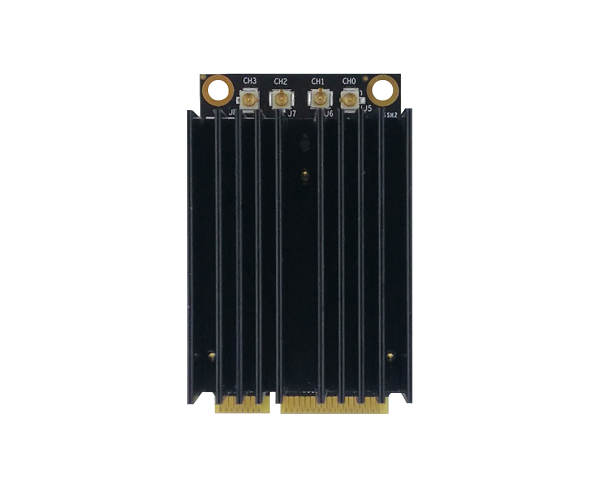
WiFi 6 4×4 MU-MIMO Dual Band Module QCN6024 WLE3000HX
- Qualcomm QCN6024 or QCN9024 ‘Pine’ series for Commercial Grade
- Qualcomm QCN9074 ‘Pine’ series for Industrial Grade
- Standard size MiniPCIe with PCIe 3.0 Interface
- Derived from PN02.1 Reference Design
- Supports up to 1024-QAM
- -20°C to 70°C operating temperature for commercial grade
- -40°C to 85°C operating temperature for industrial grade
Description
WLE3000HX is a Dual-Band Selectable (2.4GHz or 5GHz) WiFi 6 (802.11ax) module. It is based on Qualcomm’s QCN6024, QCN9024, or QCN9074 ‘Pine’ series radio solution. This is the first 4T4R (4×4) MU-MIMO 2.4GHz or 5GHz solution and is available in both commercial grade (QCN6024 or QCN9024) and industrial grade (QCN9074). Furthermore, WLE3000HX features a standard 30 x 51 mm dimension, making the hardware integration as seamless as possible. With 4 spatial streams, WLE3000HX is capable of achieving up to 4.8Gbps with the availability of 160MHz bandwidth.
WLE3000HX can deliver up to 20dBm per chain for 5GHz and 2.4GHz, and this is a perfect solution for customers who need to change frequency bands depending on their field applications. WLE3000HX is capable of doing both AP and STA mode, in this case, doing backhaul and providing connectivity for clients at the same time. Based on a 3.3V design, WLE3000HX ensures that the signal coverage is as wide as possible, and consumes less power when compared to Qualcomm’s reference design. WLE3000HX is suitable for customers who are conscious of the power consumption of their products.
Supporting up to 4096 QAMs, WLE3000HX with its OFDMA feature is a perfect solution for Enterprise, Industrial, Cybersecurity, Transportation, and SMB applications or appliances. FIPS L2 is available as a feature uniquely on QCN9074, for customers who care most about the cryptographic protection of their product. Furthermore, with Compex acting as a value-added manufacturer, WLE3000HX is not restricted to working just on Qualcomm’s ecosystem, but also on 3rd party platforms such as Intel x86 and other ARM processors such as NXP and Marvell.

Standard
| Chipset(s) | Qualcomm QCN6024 Qualcomm QCN9024 Qualcomm QCN9074 |
| Type of Connector(s) | 4x U.FL Connectors |
| WiFi Interface | PCIe 3.0 |
Wireless
| Wireless | 2.4GHz 802.11b/g/n/ax, max 20dBm per chain 5GHz 802.11a/n/ac/ax, max 20dBm per chain |
| 2.4GHz | 4×4 MU-MIMO, up to 1376.4Mbps |
| 5GHz | 4×4 MU-MIMO, up to 4804Mbps |
| WLAN Frequency Range | 2.412~2.472GHz 5.150~5.850GHz |
| Channel Spectrum Widths for WLAN | 20/40MHz at 2.4GHz 20/40/80/160MHz at 5GHz |
Power
| Power Consumption | 9W (Max) |
| Operating Voltage | 3.3V |
Certifications
| FCC (USA) | FCC |
| CE RED (EU Region) | CE RED |
| IC (Canada) | IC |
Environmental Compliances
| USA | REACH |
| EU Region | RoHS |
Hardware Architecture
Component Map Overview
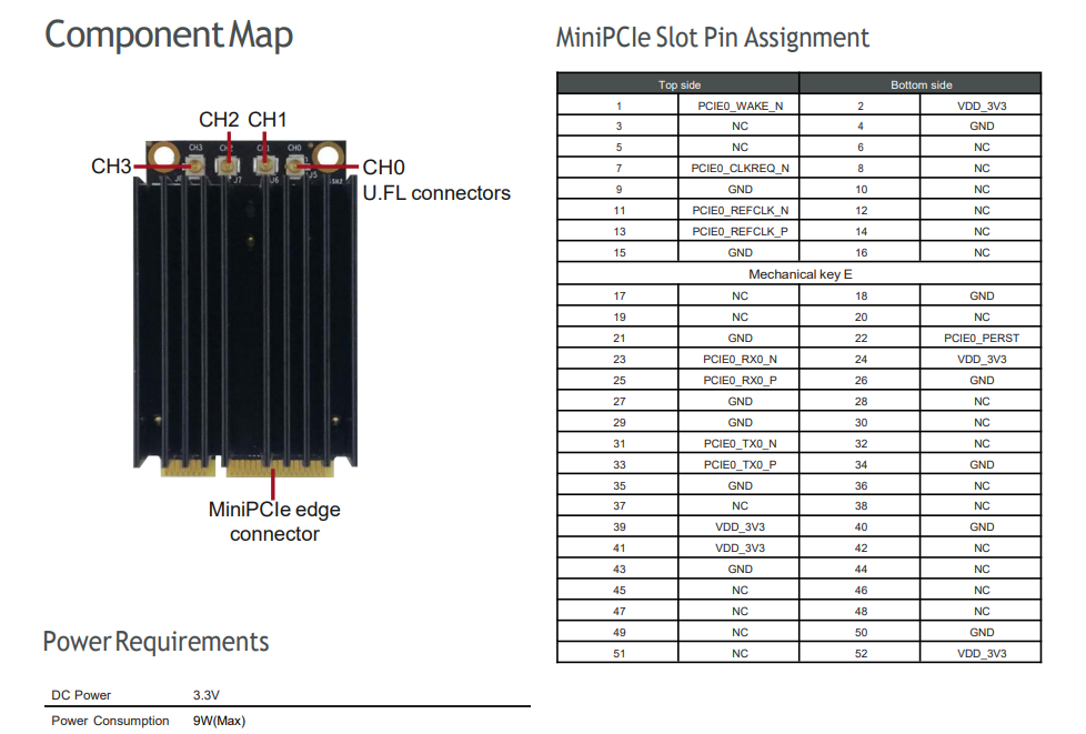
The WLE3000HX module features a compact 30 x 51 mm form factor with an optimized component layout designed for high-performance wireless communication. The module incorporates four U.FL connectors (CH0, CH1, CH2, CH3) enabling 4×4 spatial stream configuration for maximum throughput and signal diversity.
Key Components
| Component | Description & Function |
| U.FL Connectors (CH0-CH3) | Four RF connectors supporting 4×4 MU-MIMO configuration. Each channel operates independently to enable spatial multiplexing, improving data throughput and signal reliability in dense environments. |
| MiniPCIe Edge Connector | Standard MiniPCIe interface providing PCIe 3.0 connectivity for high-speed data transfer between the module and host system. Supports plug-and-play integration with compatible motherboards. |
| Heat Sink | Integrated thermal management solution ensuring optimal operating temperatures during high-bandwidth operations, preventing thermal throttling and maintaining consistent performance. |
MiniPCIe Slot Pin Assignment
The WLE3000HX utilizes a standard MiniPCIe interface with 52 pins, providing power, ground, and high-speed differential signaling for PCIe 3.0 communication. Below is the complete pin assignment specification:
| Pin Number | Top Side Signal | Bottom Side Signal |
|---|---|---|
| 1 | PCIE0_WAKE_N | VDD_3V3 |
| 2 | NC | NC |
| 3 | NC | GND |
| 4 | NC | NC |
| 5 | PCIE0_CLKREQ_N | NC |
| 6 | GND | NC |
| 7 | PCIE0_REFCK_N | NC |
| 8 | PCIE0_REFCK_P | GND |
| 9 | GND | NC |
| 10 | NC | NC |
| Mechanical Key E | ||
| 17 | NC | GND |
| 18 | NC | NC |
| 19 | GND | PCIE0_PERST |
| 20 | NC | NC |
| 21 | GND | PCIE0_PERST |
| 22 | PCIE0_RX0_N | VDD_3V3 |
| 23 | PCIE0_RX0_P | GND |
| 24 | GND | NC |
| 25 | NC | NC |
| 26 | GND | NC |
| 27 | NC | NC |
| 28 | NC | NC |
| 29 | GND | NC |
| 30 | PCIE0_TX0_N | GND |
| 31 | PCIE0_TX0_P | NC |
| 32 | GND | NC |
| 33 | NC | NC |
| 34 | NC | GND |
| 35 | GND | NC |
| 36 | NC | NC |
| 37 | NC | NC |
| 38 | VDD_3V3 | GND |
| 39 | VDD_3V3 | NC |
| 40 | GND | NC |
| 41 | NC | NC |
| 42 | NC | NC |
| 43 | GND | NC |
| 44 | NC | NC |
| 45 | NC | NC |
| 46 | NC | NC |
| 47 | NC | NC |
| 48 | NC | NC |
| 49 | NC | GND |
| 50 | NC | NC |
| 51 | NC | NC |
| 52 | NC | VDD_3V3 |
Pin Signal Definitions
| Signal Name | Description |
| VDD_3V3 | +3.3V DC power supply input for module operation |
| GND | Ground reference |
| PCIE0_WAKE_N | PCIe wake signal (active low) for power management events |
| PCIE0_CLKREQ_N | PCIe clock request signal (active low) |
| PCIE0_REFCK_N/P | Differential reference clock input (100MHz) |
| PCIE0_PERST | PCIe reset signal (active low) |
| PCIE0_RX0_N/P | Differential receive pair for PCIe lane 0 |
| PCIE0_TX0_N/P | Differential transmit pair for PCIe lane 0 |
| NC | Not connected – reserved for future use |
Power Requirements
The WLE3000HX module is designed with efficient power management to minimize energy consumption while delivering high-performance wireless connectivity. The following specifications detail the power requirements:
| Parameter | Specification |
| DC Input Voltage | 3.3V DC (±5% tolerance) |
| Maximum Power Consumption | 9W (Typical: 6-7W under normal operation) |
| Power Efficiency | Optimized 3.3V design reduces power consumption compared to standard 1.8V/3.3V dual-supply architectures |
Power Management Features
- Dynamic Voltage Scaling (DVS): Automatically adjusts core voltage based on processing load to optimize power efficiency
- PCIe ASPM (Active State Power Management): Supports L0s and L1 power states for reduced idle power consumption
- Wake-on-WLAN: Enables remote wake-up functionality for energy-efficient network monitoring
- Advanced Sleep Modes: Supports multiple low-power states including Deep Sleep and Hibernation modes
Application Use Cases
The WLE3000HX module is engineered for demanding wireless applications requiring high throughput and reliable connectivity. Its robust design makes it suitable for the following use cases:
- Enterprise Wireless Access Points: High-density deployments requiring 4×4 MU-MIMO for maximum client capacity
- Industrial IoT Gateways: Reliable connectivity in harsh environments with extended temperature range (industrial grade QCN9074)
- Security Appliances: FIPS L2 cryptographic support for secure wireless communications
- Transportation Systems: In-vehicle connectivity with robust signal handling for mobile environments
- SMB Networks: Cost-effective high-performance wireless solutions for small-to-medium businesses
- Backhaul Applications: Simultaneous AP/STA mode for wireless backhaul and client connectivity
Technical Advantages
| Feature | Benefit | Application Impact |
| 4×4 MU-MIMO | Four spatial streams for parallel data transmission | Increased network capacity and reduced latency in dense environments |
| 160MHz Bandwidth | Double the channel width of standard 80MHz solutions | Maximum data rates up to 4.8Gbps for bandwidth-intensive applications |
| OFDMA Technology | Orthogonal Frequency Division Multiple Access | Efficient multi-user communication with reduced interference |
| 4096 QAM | Higher modulation scheme for increased data density | Improved spectral efficiency and throughput performance |
| Dual-Band Selectable | Switchable 2.4GHz or 5GHz operation | Flexible deployment based on environmental conditions and application requirements |
| Cross-Platform Support | Compatible with Qualcomm, Intel x86, NXP, and Marvell platforms | Seamless integration into diverse hardware ecosystems |
Q: What chipsets are supported by WLE3000HX??
WLE3000HX supports Qualcomm QCN6024, QCN9024 (commercial grade), and QCN9074 (industrial grade).
Q: Is WLE3000HX dual-band capable??
Yes, it is a dual-band selectable module that can work on 2.4GHz or 5GHz band according to application requirements.
Q: What is the MIMO configuration and maximum speed??
It uses 4×4 MU-MIMO (4T4R). The maximum rate is 1376.4Mbps on 2.4GHz and up to 4804Mbps (4.8Gbps) on 5GHz with 160MHz bandwidth.
Q: Does WLE3000HX support AP and STA mode at the same time??
Yes, it supports both AP and STA modes, enabling wireless backhaul and client access simultaneously.
Q: What is the power supply and power consumption??
Operating voltage is 3.3V DC. Maximum power consumption is 9W, typical power is 6–7W under normal operation.
Q: How many antenna connectors does WLE3000HX have??
It is equipped with 4× U.FL antenna connectors to support 4×4 MU-MIMO spatial streams.
Q: Does the QCN9074 version support FIPS L2 encryption??
Yes, FIPS L2 cryptographic security function is unique to the industrial-grade QCN9074 version.
Q: What certifications does WLE3000HX have??
It has FCC, CE RED, IC certifications, and complies with RoHS and REACH environmental standards.
Q: What interface does WLE3000HX use??
It uses a standard MiniPCIe 52-pin slot with PCIe 3.0 high-speed interface.
Is WLE3000HX dual-band capable?
Yes, it is a dual-band selectable module that can work on 2.4GHz or 5GHz band according to application requirements.
What is the MIMO configuration and maximum speed?
It uses 4×4 MU-MIMO (4T4R). The maximum rate is 1376.4Mbps on 2.4GHz and up to 4804Mbps (4.8Gbps) on 5GHz with 160MHz bandwidth.
Does WLE3000HX support AP and STA mode at the same time?
Yes, it supports both AP and STA modes, enabling wireless backhaul and client access simultaneously.
What is the power supply and power consumption?
Operating voltage is 3.3V DC. Maximum power consumption is 9W, typical power is 6–7W under normal operation.
How many antenna connectors does WLE3000HX have?
It is equipped with 4× U.FL antenna connectors to support 4×4 MU-MIMO spatial streams.
Does the QCN9074 version support FIPS L2 encryption?
Yes, FIPS L2 cryptographic security function is unique to the industrial-grade QCN9074 version.
What certifications does WLE3000HX have?
It has FCC, CE RED, IC certifications, and complies with RoHS and REACH environmental standards.
What interface does WLE3000HX use?
It uses a standard MiniPCIe 52-pin slot with PCIe 3.0 high-speed interface.


