Key RF Design Principles for Wireless AP Motherboard PCB Layout
Blog 2026-06-01
Key RF Design Principles for Wireless AP Motherboard PCB Layout
Key Overview
Who this article is for: Embedded engineers, hardware development teams, PCB design engineers, OEM/ODM procurement specialists, and technical decision-makers responsible for wireless AP motherboard PCB layout and RF design.
Core Issue: How PCB layout affects RF performance in wireless APs, including key principles for RF routing, ground plane design, power noise control, and signal isolation.
Key Conclusions: PCB layout is critical to RF performance success. 50Ω impedance control, complete ground planes, power noise control, and signal isolation must be addressed during layout. Using reference designs and checklists significantly reduces rework costs—greater investment upfront means easier debugging later.
PCB layout for wireless AP motherboards is not just about placing components. RF routing, ground design, power integrity, and digital signal isolation all directly impact final wireless performance. If these aren’t addressed during layout, later debugging typically only increases rework costs. As a core component of how to balance RF performance and cost in wireless AP motherboard development, PCB layout determines the upper limit of RF performance. Why is PCB layout so critical to RF performance? What are the core principles for RF routing and ground plane design? How does power noise affect RF performance? How should high-frequency and digital signals be isolated? What common layout mistakes exist and how can they be avoided? How can rework costs be reduced during layout? This article systematically answers these questions.
Why PCB Layout Directly Affects Wireless Performance
PCB layout impacts RF performance across multiple dimensions:
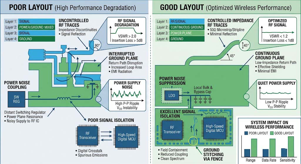
- Impact of RF trace impedance control (50Ω) on reflection and loss: RF signals are extremely sensitive to impedance. Mismatched impedance causes signal reflection, increased loss, and directly affects transmit power and receive sensitivity. Impedance control requires precise calculation during PCB stackup design.
- Antenna impedance shift and reduced radiation efficiency from incomplete ground planes: Ground planes provide return paths for RF signals. Incomplete ground planes cause impedance shifts, reduced radiation efficiency, and even impact antenna design effectiveness.
- Power supply noise coupling to RF links, affecting EVM and transmit quality: Power supply noise couples into RF links, reducing EVM (Error Vector Magnitude) and affecting higher-order modulation performance.
- Impact of digital noise on receive sensitivity: High-speed digital signal switching generates noise that couples into RF receive chains, reducing sensitivity.
These impacts demonstrate that PCB layout isn’t simply a “routing” problem—it’s a core component of RF system design.
Basic Principles of RF Routing
RF routing is the most critical aspect of PCB layout and requires following these principles:
- Impedance control (50Ω) and stackup design: RF traces must precisely maintain 50Ω impedance, requiring careful calculation during PCB stackup design considering trace width, dielectric thickness, and permittivity. Use professional impedance calculation tools (e.g., Polar SI9000).
- Minimize trace length to reduce loss: RF signals lose power in traces—shorter traces minimize attenuation.
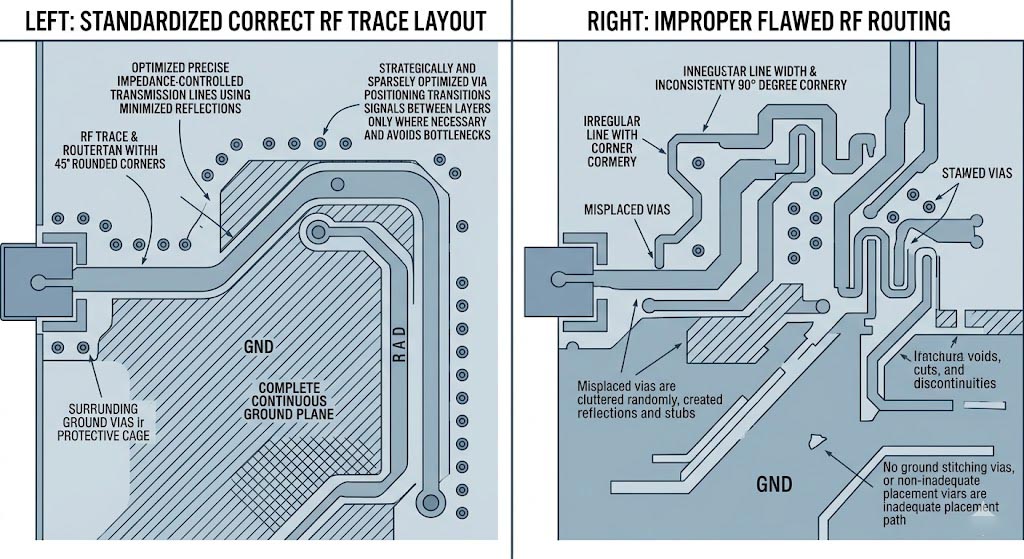
- Avoid right-angle turns; use arcs or 45° angles: Right-angle turns cause impedance discontinuities and reflections. Use arcs or 45° angles to maintain impedance continuity.
- Minimize via count (vias introduce parasitic inductance and capacitance): Vias introduce parasitic elements that affect impedance matching. Minimize vias on RF traces—use blind/buried vias when necessary.
- Maintain complete ground plane under RF traces; avoid crossing splits: RF traces must have a continuous ground plane beneath them as a return path. Crossing ground plane splits causes impedance discontinuities and radiation.
- Separate RF traces from digital signals, clocks, DC-DC converters, and other noise sources: Digital signals and power supply noise couple into RF traces, degrading performance. Maintain sufficient distance (typically ≥ 3mm).
| Principle | Purpose | Consequences of Violation |
|---|---|---|
| 50Ω Impedance Control | Avoid reflections, ensure signal integrity | Deteriorated VSWR, reduced transmit power |
| Minimize Trace Length | Reduce loss | Signal attenuation, reduced sensitivity |
| Avoid Right-Angle Turns | Maintain impedance continuity | Impedance discontinuity, increased reflection |
| Minimize Vias | Reduce parasitic parameters | Impedance shift, matching difficulties |
| Continuous Ground Plane | Ensure return path | Impedance shift, reduced radiation efficiency |
| Isolate from Noise Sources | Avoid noise coupling | Noise interference, degraded performance |
What to Consider for Ground Plane Design
Ground plane design is central to RF PCB layout:
- Ground planes must be continuous—avoid splits and gaps: Ground planes provide return paths for RF signals. Splits and gaps force return paths to detour, increasing inductance and impedance.
- Maintain complete ground plane under RF traces; avoid crossing splits: RF traces require continuous ground beneath them. Crossing splits causes impedance discontinuities and radiation.
- Use dedicated ground layers in multi-layer boards: In multi-layer designs, use a dedicated ground layer (typically Layer 2) to ensure ground plane integrity and low impedance.
- Connect RF component ground pins to ground layer with multiple vias: RF components need multiple vias connecting ground pins to the ground layer to reduce ground impedance and improve heat dissipation.
- Handle ground plane in antenna areas (clearance zones, antenna islands): Antenna areas require special ground plane treatment such as clearance zones or antenna islands—see antenna design guide for details.
How Power Noise Affects RF Performance
Power supply noise impact on RF performance is often underestimated:
- DC-DC switching noise impact on RF transmit and receive: DC-DC switching noise couples into RF links, affecting transmit EVM and receive sensitivity. Pre-testing before EMC certification is recommended.
- LDO vs DC-DC selection for RF power: LDOs have low noise but lower efficiency; DC-DCs have higher efficiency but more noise. For noise-sensitive RF circuits, use LDOs or low-noise DC-DCs.
- Power decoupling capacitor placement and value selection: Decoupling capacitors must be placed close to component pins, with appropriate value combinations (large capacitors for low frequencies, small capacitors for high frequencies).
- Isolate power traces from RF traces: Power traces should be routed away from RF traces to prevent noise coupling.
- Power plane and ground plane coupling design: Tightly couple power and ground planes to reduce power impedance and improve power integrity.
| Power Solution | Noise Level | Efficiency | Application Scenario |
|---|---|---|---|
| LDO | Low (< 10μVrms) | Low (60-80%) | Noise-sensitive RF circuits |
| Low-Noise DC-DC | Medium (< 50μVrms) | High (85-95%) | Circuits with moderate noise requirements |
| Standard DC-DC | High (< 100μVrms) | High (85-95%) | Digital circuits, non-critical RF circuits |
How to Isolate High-Frequency and Digital Signals
Isolating high-frequency and digital signals is a key challenge in RF PCB layout:
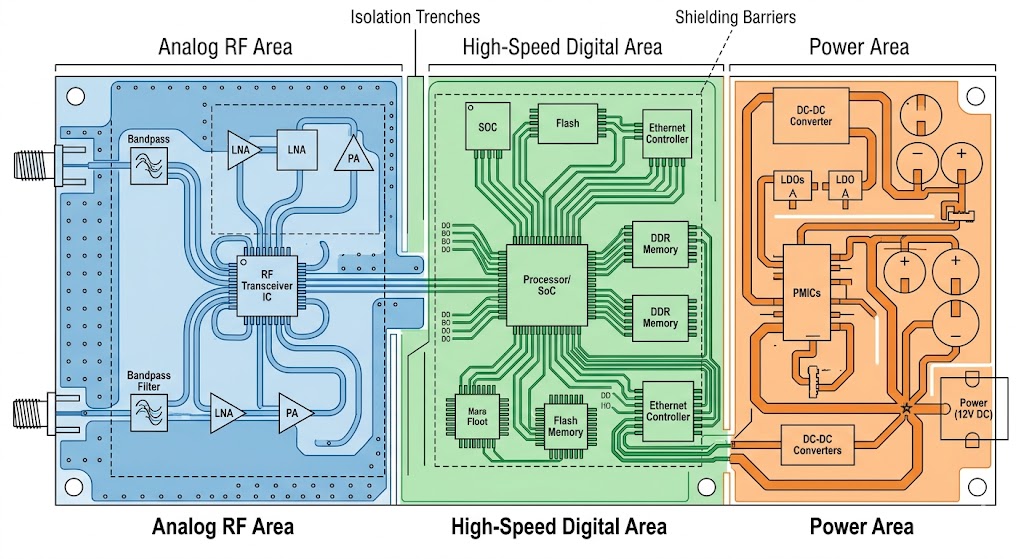
- PCB zoning: clearly separate RF, digital, and power regions: During layout, clearly define RF, digital, and power zones to prevent cross-interference.
- Ground isolation: single-point connection between RF ground and digital ground: Connect RF ground and digital ground at a single point (typically at power entry) to avoid ground loop noise.
- Trace isolation: maintain distance between RF and digital traces, avoid long parallel runs: RF and digital traces must maintain sufficient separation and avoid parallel routing that causes coupling.
- Use shielding cans over RF regions: Enclose RF regions with metal shielding cans to isolate external interference.
- Clock signals should be routed away from RF regions; add shielding or filtering if necessary: Clock signals are major noise sources—route them away from RF areas and add filtering when needed.
| Isolation Measure | Purpose | Implementation Key Points |
|---|---|---|
| PCB Zoning | Avoid cross-interference | Clearly define RF, digital, and power zones |
| Ground Isolation | Avoid ground loop noise | Single-point connection between RF and digital ground |
| Trace Isolation | Avoid coupling | Maintain distance, avoid long parallel traces |
| Shielding Cans | Isolate external interference | Use metal shielding cans over RF regions |
| Clock Filtering | Reduce clock noise | Route clocks away from RF areas, add filtering |
Common Layout Mistakes
Common PCB layout mistakes include:
- RF traces crossing ground plane splits: Causes impedance discontinuity, degraded VSWR, and reduced transmit power.
- RF traces that are too long or have excessive vias: Increases signal loss, impedance shift, and matching difficulties.
- Incomplete ground planes, insufficient vias at RF component ground pins: Increases ground impedance, reduces radiation efficiency, and impairs heat dissipation.
- DC-DC converters placed near RF components, causing severe noise coupling: Increases RF noise, degrades EVM, and reduces sensitivity.
- Antenna clearance zones encroached by ground or components: Causes antenna impedance shift and reduced radiation efficiency—see antenna design guide for more details.
- Power decoupling capacitors placed too far from component pins: Reduces decoupling effectiveness and increases power noise.
- Clock signals routed near RF regions: Causes clock noise to couple into RF links, degrading performance.
These mistakes are often discovered only during later debugging, at which point modifications are extremely costly. Therefore, strict adherence to layout guidelines during the design phase is essential.
How to Reduce Rework Costs During Layout
Key strategies to reduce rework costs:
- Define RF architecture and stackup from requirements phase: Determine RF architecture, PCB layer count, and stackup early in the project to avoid major later modifications.
- Start with reference designs: Chip vendors’ reference designs have been validated and can serve as a starting point to reduce risk.
- Plan stackup and RF trace paths before layout: Plan RF trace routes, ground plane splits, and power routing before beginning layout to avoid later conflicts.
- Use simulation tools (electromagnetic simulation, SI/PI analysis) to identify risks early: Use tools like HFSS, CST for electromagnetic simulation and SI/PI tools to detect impedance matching, signal integrity, and power integrity issues upfront.
- Reserve space for matching network tuning (L/C positions): Leave space near RF traces for matching networks (inductors, capacitors) to facilitate later debugging.
- Use layout checklists for verification: Employ standardized checklists to ensure critical design points aren’t overlooked.
- Collaborate early with RF engineers and mechanical engineers: Engage RF and mechanical engineers during layout to avoid later conflicts.
| Early Investment | Late Rework Cost |
|---|---|
| Stackup planning: 1-2 days | Redesign: 2-4 weeks + $5,000-20,000 |
| Simulation validation: 2-3 days | Debug failures: 1-2 weeks + $2,000-10,000 |
| Checklist verification: 0.5 days | Missed issues: 1-3 weeks + $3,000-15,000 |
| Team collaboration: 1-2 days | Conflict resolution: 1-2 weeks + $2,000-8,000 |
Layout Checklist
Use the following checklist for verification:
| Item | Requirements | Status |
|---|---|---|
| RF traces implement 50Ω impedance control | Verify with impedance calculation tool | ✅ / ❌ |
| RF traces are short, direct, with minimal vias | Visual inspection, simulation if necessary | ✅ / ❌ |
| RF traces have continuous ground plane beneath | Check ground plane continuity | ✅ / ❌ |
| RF component ground pins have sufficient vias | At least 2-4 vias per ground pin | ✅ / ❌ |
| DC-DC converters are positioned away from RF areas | Distance ≥ 10mm | ✅ / ❌ |
| Antenna clearance zones meet requirements | Refer to antenna design specifications | ✅ / ❌ |
| Power decoupling capacitors are close to component pins | Distance < 5mm | ✅ / ❌ |
| RF and digital zones are clearly separated | No cross-interference | ✅ / ❌ |
| Clock signals are routed away from RF areas | Distance ≥ 10mm | ✅ / ❌ |
| Space reserved for matching network tuning | L/C positions near each RF trace | ✅ / ❌ |
Summary
PCB layout is critical to RF design success in wireless APs:
- PCB layout determines RF design success: RF routing, ground planes, power noise, and signal isolation all require systematic planning.
- RF routing, ground planes, power noise, and signal isolation require systematic planning: It’s not simply a “routing” problem but a core component of RF system design.
- Most mistakes stem from inadequate early planning: Strict adherence to guidelines during layout prevents costly later modifications.
- Reference designs and checklists significantly reduce rework costs: Validated reference designs and standardized checklists ensure critical design points aren’t missed.
- Greater upfront investment means easier debugging later: Early investment in planning and verification is far less costly than fixing issues post-production.
In practice, wireless AP motherboard RF routing, PCB ground plane design, power noise control, and layout checklists are all critical considerations. As a core component of how to balance RF performance and cost in wireless AP motherboard development, PCB layout must be coordinated with antenna design, EMC certification, and mass production debugging to achieve optimal performance-cost balance.
References
Frequently Asked Questions
Q: What are the most critical RF design considerations in wireless AP motherboard PCB layout?
The most critical RF design points include: 1) 50Ω impedance control: RF traces must precisely maintain 50Ω impedance as the foundation for signal integrity; 2) Continuous ground plane: RF traces require continuous ground beneath them as a return path—crossing splits causes impedance discontinuity; 3) Power noise control: Decoupling capacitors must be placed close to component pins to prevent noise coupling into RF links; 4) Signal isolation: RF traces must be separated from digital signals and clocks to avoid noise interference.
Q: Can RF traces cross ground plane splits?
Absolutely not. RF traces require a continuous ground plane beneath them as a return path. Crossing splits causes impedance discontinuity, degraded VSWR, and reduced transmit power. If crossing is unavoidable, use bridging capacitors or traces—but this increases complexity and cost. The best practice is to plan RF trace paths during layout to avoid crossing splits.
Q: How significant is DC-DC power supply impact on RF performance, and how can it be mitigated?
DC-DC power supplies significantly impact RF performance: switching noise couples into RF links, degrading EVM and receive sensitivity. Mitigation strategies include: 1) Selecting low-noise DC-DCs or using LDOs; 2) Locating DC-DCs away from RF areas (≥ 10mm recommended); 3) Adding LC filtering at DC-DC outputs; 4) Isolating power traces from RF traces; 5) Pre-testing before EMC certification to ensure noise levels are acceptable.


