How to Balance RF Performance and Cost in Wireless AP Motherboard Development
Blog 2026-06-01
How to Balance RF Performance and Cost in Wireless AP Motherboard Development
Key Overview
Who this article is for: Embedded engineers, hardware development teams, OEM/ODM procurement specialists, and technical decision-makers responsible for wireless AP motherboard design and selection.
Core Issue: How to meet RF performance requirements while controlling BOM costs, certification costs, and mass production debugging costs in wireless AP motherboard development.
Key Conclusions: Performance and cost in wireless AP motherboards require system-level trade-offs. Clear scenario definition and target specifications are essential. Implement modular design, tiered product strategies, and prioritize critical paths while considering both performance and cost at every stage from requirements to mass production.
Wireless AP motherboard development isn’t just about component selection and board layout. The real determinant of product success is often the balance between RF performance and cost. For home, commercial, and enterprise-grade products, performance targets, certification requirements, and production budgets differ significantly. Only by considering all these factors together can you create a solution that’s both reliable and competitive. Why is balancing performance and cost so difficult? What are the key cost drivers? How should trade-offs be made across different product types? What practical strategies and common pitfalls exist? This article systematically addresses these questions.
Why Balancing Performance and Cost is So Challenging
Balancing performance and cost in wireless AP motherboards is challenging due to three core factors:
- RF circuits are extremely sensitive to materials, components, and PCB layer count: RF signals are highly sensitive to impedance, loss, and noise. Even minor design changes can significantly impact performance. Achieving better performance typically requires higher-spec components, more PCB layers, and superior materials, leading to non-linear cost increases.
- Certification requirements (CE/FCC/EMC) impact design and testing costs: Different markets and product types have varying certification requirements. Certification failures lead to redesigns, delays, and additional testing costs. As discussed in EMC Certification for Wireless APs, many projects incur significant additional costs due to inadequate early-stage certification planning.
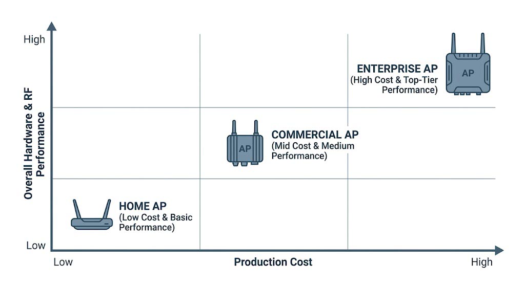
- Differing performance/cost targets across home, commercial, and enterprise products: Home APs prioritize price and ease of use, enterprise APs prioritize performance and reliability, while commercial APs need to balance both. Products with different positioning require entirely different performance targets and cost budgets, ruling out a one-size-fits-all design approach.
These three factors intersect, making performance-cost balance a systems engineering challenge rather than a simple component selection problem.
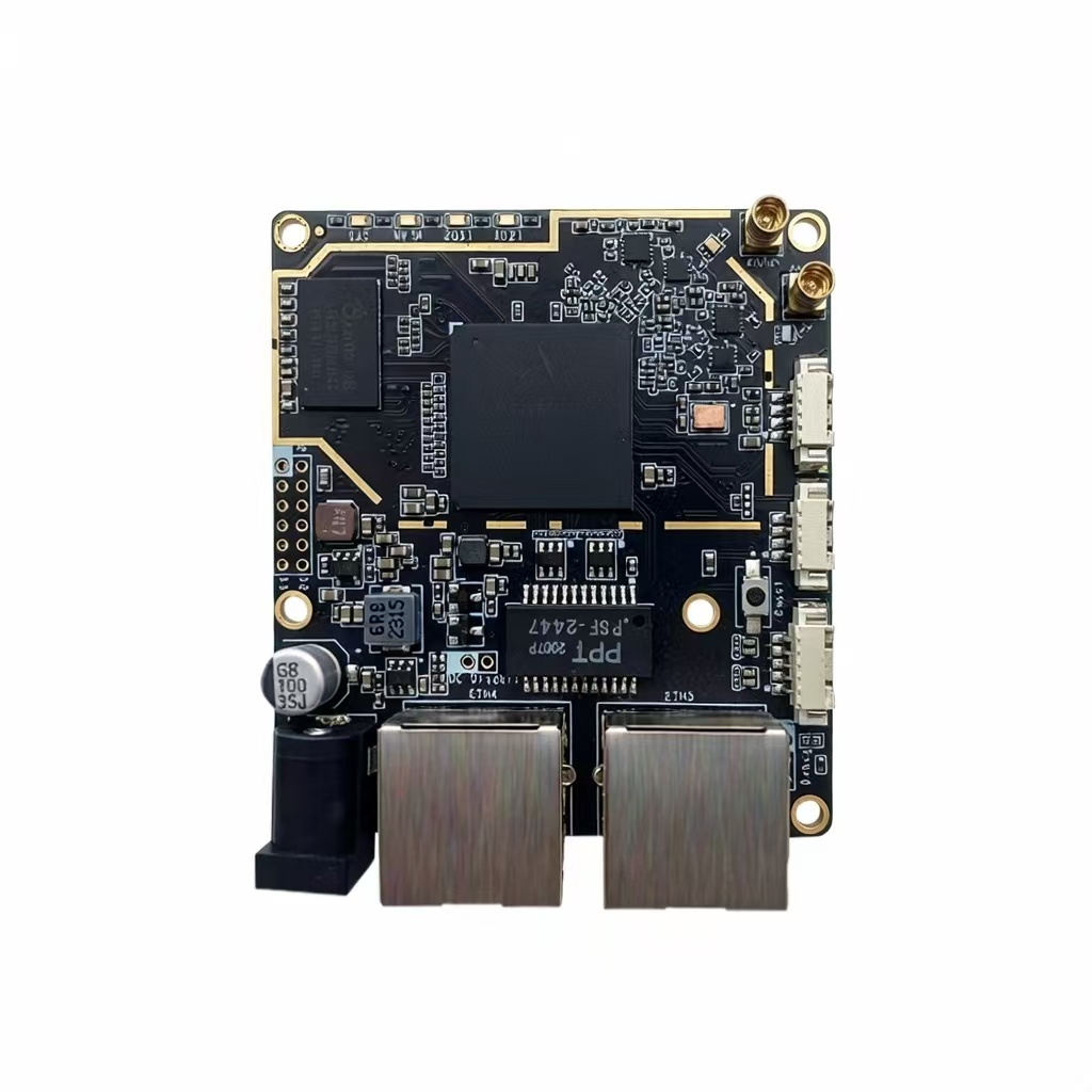
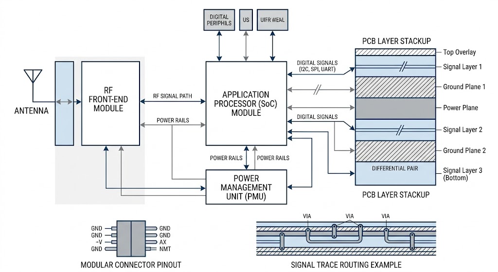
Core Components of Wireless AP Motherboards
To balance performance and cost effectively, first understand the core components of wireless AP motherboards:
| Module | Function | Performance Impact | Cost Impact |
|---|---|---|---|
| Wi-Fi SoC / Chipset | Core processing unit with integrated MAC/PHY/RF | Determines maximum throughput, MIMO capability, protocol support | High (20-30% of BOM) |
| RF Front-end (PA/LNA/Switch/FEM) | Signal amplification, filtering, switching | Determines transmit power, receive sensitivity, linearity | High (15-25% of BOM) |
| Antenna Design (On-board/External/MIMO) | Electromagnetic wave radiation and reception | Determines coverage range, signal quality, MIMO gain | Medium to High (depending on antenna type and count) |
| Power Management (LDO/DC-DC) | Power supply and noise control | Affects RF noise, EVM, stability | Medium (5-10% of BOM) |
| PCB Layers and Materials | RF routing, impedance control, ground plane | Affects RF loss, impedance matching, EMC | High (significant impact from layers and materials) |
| Passive Components (Matching Networks, Filters) | Impedance matching, filtering | Affects RF matching, filtering effectiveness | Low to Medium |
Each module selection impacts the performance-cost balance. For example, choosing a highly integrated SoC reduces peripheral components but may sacrifice some performance; selecting external high-gain antennas improves coverage but increases cost and size. For more details on antenna design and PCB layout, refer to the dedicated articles.
How RF Performance Impacts User Experience
RF performance isn’t an abstract technical specification; it directly impacts user experience:
- Coverage range and signal strength: Transmit power and antenna gain determine coverage. Insufficient signal strength causes unstable connections and reduced speeds at the edges.
- Throughput, latency, and stability: RF link quality determines actual throughput and latency. Poor performance leads to video buffering, gaming lag, and slow file transfers.
- Multi-device concurrency: MIMO and concurrent processing capabilities determine the experience when multiple devices connect simultaneously. Insufficient capacity causes interference and speed degradation.
- Roaming experience and disconnection rate: For enterprise APs, roaming performance determines how well mobile devices switch between APs. Poor roaming causes dropped connections.
Major Cost Components of Wireless AP Motherboards
Understanding cost structure is essential for balancing performance and cost:
| Cost Item | Percentage of BOM | Key Influencing Factors |
|---|---|---|
| Chipset (SoC) | 20–30% | Performance grade, integration level, protocol support |
| RF Front-end Components (PA/LNA/Switch/FEM) | 15–25% | Power rating, linearity, number of frequency bands |
| PCB (Layers, Materials, Process) | 10–20% | Layer count, materials, impedance control requirements |
| Antenna (On-board/External, MIMO Count) | 5–15% | Antenna type, quantity, gain |
| Passive Components & Matching Networks | 3–8% | Precision requirements, quantity |
| Certification & Testing (CE/FCC/EMC/Radio) | 5–10% (one-time) | Certification type, number of tests |
| Mass Production Debugging & Yield Costs | 5–10% | Debug complexity, yield rate |
From this breakdown, chipset, RF front-end, and PCB are the three major cost drivers. For more on BOM cost optimization, refer to the dedicated article.
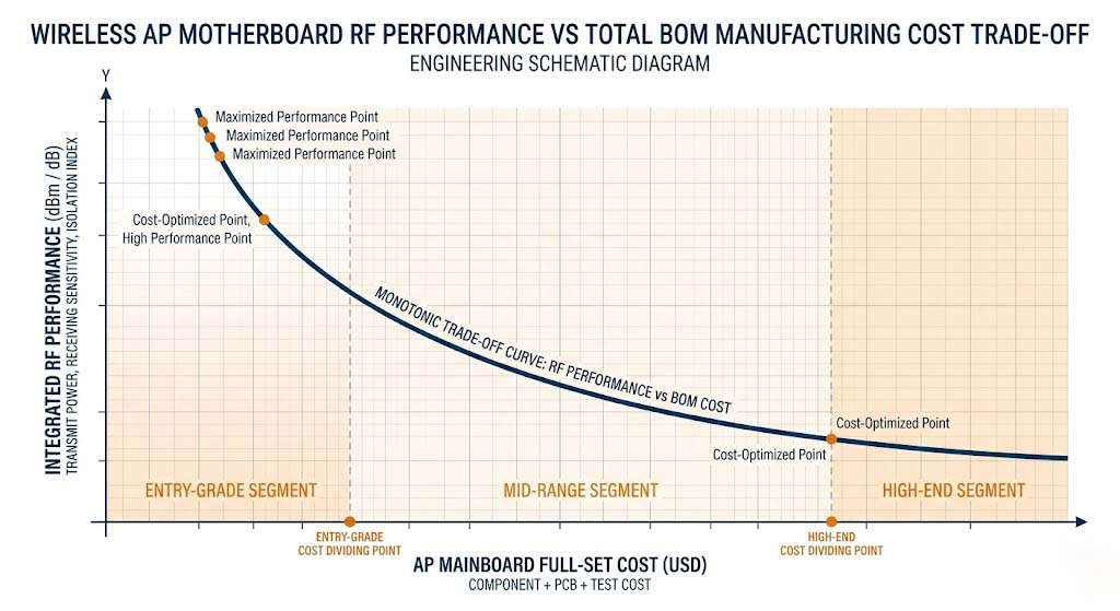
Where Performance and Cost Conflict
Key conflicts between performance and cost include:
| Performance Improvement Direction | Corresponding Cost Increase |
|---|---|
| Higher-order modulation (256-QAM → 1024-QAM) | Requires higher linearity PA, 20-40% cost increase |
| Increased MIMO streams (2×2 → 4×4) | Doubles RF front-end components, increases PCB complexity, 50-100% cost increase |
| External high-gain antennas | Increases antenna cost and structural complexity, 30-50% cost increase |
| Multi-layer PCB + high-frequency materials | 40-80% cost increase (4-layer → 6-layer) |
| Stricter EMC/RF specifications | Increases filter, shielding, and testing costs by 20-40% |
These conflicts demonstrate that performance improvements rarely scale linearly with cost—they often grow exponentially. Therefore, clearly defining “must-have” vs. “nice-to-have” performance is critical.
—
【Image Placeholder Start】
– Image Position: After H2 “Where Performance and Cost Conflict”
– Visual Concept: Chart showing cost increase vs. performance improvement for different enhancement directions
– AI Prompt: Chart showing cost increase vs performance improvement in wireless AP development, with different curves for MIMO upgrade, modulation upgrade, and PCB layer increase, professional business style
【Image Placeholder End】
—
Strategies for Balancing RF Performance and Cost
Core strategies for balancing performance and cost:
- Define target scenarios and performance metrics (home/commercial/enterprise): Different scenarios have different performance baselines—don’t pay for performance you don’t need.
- Define “must-have” vs. “acceptable” performance: Prioritize performance on critical frequency bands (e.g., 5GHz) and paths; allow reasonable trade-offs on secondary paths.
- Implement modular design (switchable PA/antenna configurations): Modular designs support different configurations, reducing BOM pressure for single SKUs.
- Adopt tiered product strategy (Standard/Pro/Enterprise): Different tiers serve different market needs, avoiding over-design.
- Prioritize critical paths, allow reasonable degradation on secondary paths: For example, use high-spec FEM on 5GHz, medium-spec on 2.4GHz.
- Optimize PCB layers and materials: Choose the lowest-cost solution that meets impedance control and loss requirements. See PCB layout optimization for details.
- Select chipset platforms appropriately (integration vs. discrete components): Highly integrated SoCs reduce peripherals but may sacrifice performance.
- Reduce post-development debugging costs through simulation and pre-testing: Early simulation investment significantly reduces later redesign and debugging costs.
| Strategy | Performance Impact | Cost Impact |
|---|---|---|
| Scenario-based performance targets | Ensures meeting actual requirements | Avoids over-design, 10-30% reduction |
| Modular design | Maintains flexibility | Reduces single-SKU BOM pressure |
| Tiered product strategy | Meets diverse needs | Optimizes overall cost structure |
| Critical path prioritization | Ensures core performance | Reduces secondary path costs by 10-20% |
| Simulation & pre-testing | Reduces later issues | Reduces debugging costs by 20-40% |
Design Strategies for Different Product Types
Different product types require different design strategies:
| Product Type | Typical Performance Targets | Typical Cost Strategy | Typical Component Selection |
|---|---|---|---|
| Home AP | Cost-sensitive, moderate performance, easy deployment | Strict BOM cost control, prioritize low-cost solutions | 2×2 MIMO SoC, on-board antenna, 4-layer PCB, mid-range FEM |
| Commercial AP | Balanced performance and cost, emphasize stability and manageability | Moderate investment, balance performance and cost | 2×2/4×4 MIMO SoC, on-board/external antenna, 4-6 layer PCB, mid-range FEM |
| Enterprise AP | Performance-first, support high concurrency and advanced features | Performance prioritized, accept higher costs | 4×4/8×8 MIMO SoC, external high-gain antenna, 6+ layer PCB, high-spec FEM |
For more on hardware design differences between home and enterprise APs, refer to the dedicated article.
Recommended Development Process
Recommended development process:
- Requirements Definition: Define scenarios, performance metrics, certification requirements, and target BOM cost
- Chipset & Platform Selection: Select appropriate platform based on performance targets and cost budget
- RF Architecture Design: Define PA/LNA/Switch/filter/antenna scheme
- PCB Stackup & Impedance Control Planning: Determine layer count, materials, impedance requirements
- Schematic & Layout: RF routing, matching networks, ground plane design
- Simulation & Pre-testing: Electromagnetic simulation, S-parameters, EVM pre-testing
- Engineering Prototype & Debugging: Functional verification, performance optimization
- Certification Testing: CE/FCC/EMC/radio certification
- Mass Production Introduction & Yield Optimization: See mass production debugging process for details
Consider both performance and cost at each stage to avoid costly late-stage redesigns.
Common Pitfalls to Avoid
Common pitfalls in performance-cost balancing:
- Chasing theoretical peak rates while ignoring real-world performance: Laboratory specs look impressive but fail to deliver in actual environments, leading to poor user experience.
- Over-specifying (premium PA/multi-layer PCB) leading to cost overruns: Paying for unnecessary performance makes products uncompetitive on price.
- Neglecting antenna design and matching networks, relying only on chip upgrades: Antenna design defines performance limits. See antenna design guide for details.
- Ignoring certification requirements early, causing costly redesigns: Certification failures lead to redesigns, delays, and significantly increased costs.
- Focusing only on unit performance while ignoring production yield and debugging costs: Lab prototypes perform well, but mass production suffers from low yield and high debugging costs.
Summary
Balancing performance and cost in wireless AP motherboards is a systems engineering challenge:
- RF performance and cost require system-level trade-offs: It’s not simply a component selection problem but requires optimization across the entire flow from requirements to mass production.
- Clear scenario definition and target metrics are essential: Different product types have different performance baselines and cost budgets.
- Modular design, tiered products, and critical path prioritization are core strategies: Flexible designs achieve optimal cost-performance ratios.
- Consider both performance and cost at every stage from requirements to production: Avoid costly late-stage changes by addressing both factors early.
In practice, wireless AP motherboard RF design, PCB layout optimization, RF front-end cost optimization, EMC certification, mass production debugging, and mechanical-electrical co-design are all critical considerations. Finding the optimal balance between performance and cost requires careful planning and execution throughout the entire development lifecycle. For product positioning guidance, see home vs enterprise AP comparison. For market strategy, see monetization strategies for wireless AP products.
References
Frequently Asked Questions
Q: What are the most critical factors affecting RF performance in wireless AP motherboard development?
The most critical factors include: 1) Linearity and noise figure of RF front-end components (PA/LNA), 2) Antenna gain and radiation efficiency, 3) PCB layout impedance control and ground plane design, and 4) Power supply noise control. Among these, RF front-end and antenna design determine performance limits, while PCB layout and power design ensure consistent performance.
Q: When cost is constrained, which RF metrics should be prioritized?
When cost is limited, prioritize: 1) Coverage and signal strength (transmit power and antenna gain), 2) Throughput and stability on core frequency bands (typically 5GHz), and 3) Basic certification requirements (CE/FCC/EMC). Secondary bands (e.g., 2.4GHz) can be moderately downgraded, or software optimization can compensate for hardware limitations.
Q: What are the main RF design differences between home and enterprise APs?
Key differences include: 1) Transmit power and receive sensitivity: Enterprise APs require higher specs, 2) MIMO capability: Enterprise APs typically support 4×4 or higher while home APs are mostly 2×2, 3) Antenna solutions: Enterprise APs use external high-gain antennas while home APs use on-board antennas, 4) PCB layers: Enterprise APs typically require 6+ layers while home APs use 4 layers, 5) Certification and testing: Enterprise APs have stricter EMC, reliability, and long-term stability requirements.
Q: How much does EMC certification typically cost for a wireless AP motherboard?
EMC certification costs vary significantly by region and product type. For a typical wireless AP, FCC testing in the US ranges from $15,000 to $30,000, CE testing in Europe ranges from $20,000 to $40,000, and combined testing for multiple markets can reach $50,000 to $80,000. These costs include radiated emission testing, conducted emission testing, immunity testing, and RF performance verification. Planning for certification early in the design phase can significantly reduce the risk of costly retesting.
Q: What PCB layer count is recommended for a dual-band wireless AP motherboard?
For a dual-band (2.4GHz + 5GHz) wireless AP motherboard, a 4-layer PCB is the minimum viable option for cost-sensitive home APs, providing adequate impedance control with proper stackup design. For commercial and enterprise APs requiring better isolation and signal integrity, 6-layer PCBs are strongly recommended. An 8-layer PCB may be necessary for tri-band or 4×4 MIMO designs. Each additional layer typically increases PCB fabrication cost by 20-30%, so layer count should be matched to performance requirements.